Wireless Chip and Electronic Device Having Wireless Chip

a technology of electronic devices and wireless chips, applied in the direction of antenna earthings, substantially flat resonant elements, resonant antennas, etc., can solve the problem of low durability and achieve the effects of high mechanical strength, control of the quality data and storage situation of products, and high durability

Inactive Publication Date: 2008-07-24
SEMICON ENERGY LAB CO LTD
View PDF15 Cites 41 Cited by
  • Summary
  • Abstract
  • Description
  • Claims
  • Application Information

AI Technical Summary

Benefits of technology

[0013]In addition, since a patch antenna has high mechanical strength, it can be used repeatedly. Therefore, it is possible to provide a container, which has high durability and is recyclable like a returnable container, with the patch antenna.
[0014]In addition, the wireless chip having a sensor device can read data, which is detected by the sensor device, with a reader / writer. Therefore, it is possible to control quality data and storage situation of products.
[0015]In addition, a wireless chip having a battery can transmit a signal to a reader / writer automatically. In addition, the communication distance with the reader / writer can be lengthened.

Problems solved by technology

Further, the wireless chip having such an antenna has a problem that durability is low.

Method used


Image

  • Wireless Chip and Electronic Device Having Wireless Chip
  • Wireless Chip and Electronic Device Having Wireless Chip
  • Wireless Chip and Electronic Device Having Wireless Chip

Examples


embodiment mode 1

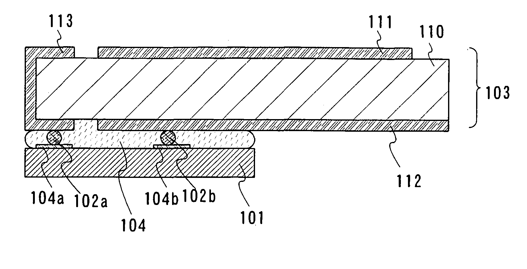
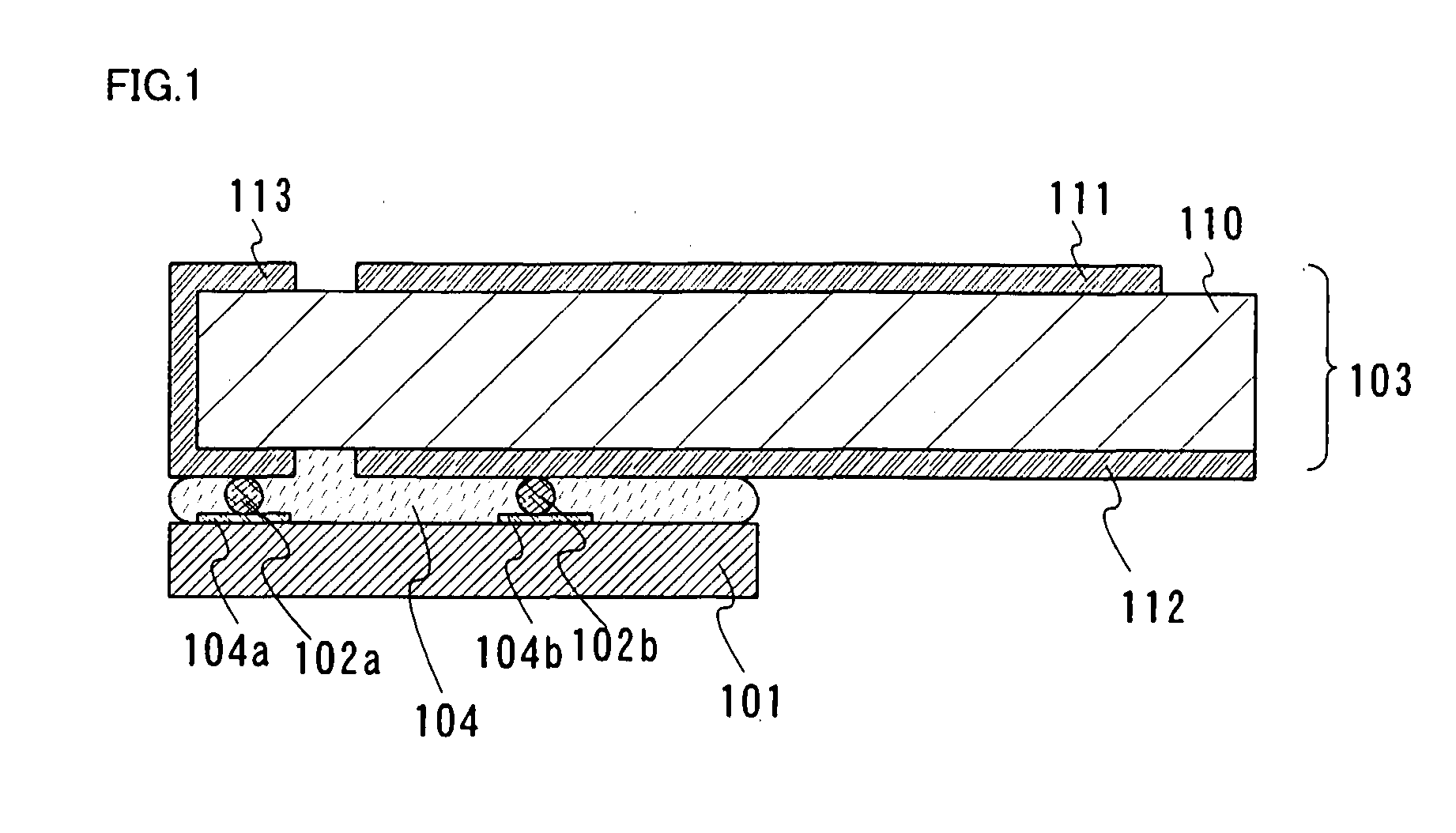
[0034]A description is made on one embodiment mode of a wireless chip of the present invention referring to FIG. 1. FIG. 1 is a cross-sectional diagram of a wireless chip.

[0035]In a wireless chip of the present embodiment mode, a chip 101 having a field-effect transistor and an antenna (hereinafter, which is described as a patch antenna 103) are connected by conductive layers 102a and 102b. Concretely, a connection terminal 104a formed over the surface of the chip 101 having a field-effect transistor and a power feeding layer 113 of the patch antenna are connected by the conductive layer 102a. In addition, a connection terminal 104b formed over the surface of the chip 101 having a field-effect transistor and a conductive layer 112 functioning as a ground contact body of the patch antenna are connected by the conductive layer 102b. In addition, a connecting portion of the patch antenna 103 and the chip 101 having a field-effect transistor may be filled with an under fill 104.

[0036]Th...

embodiment mode 2

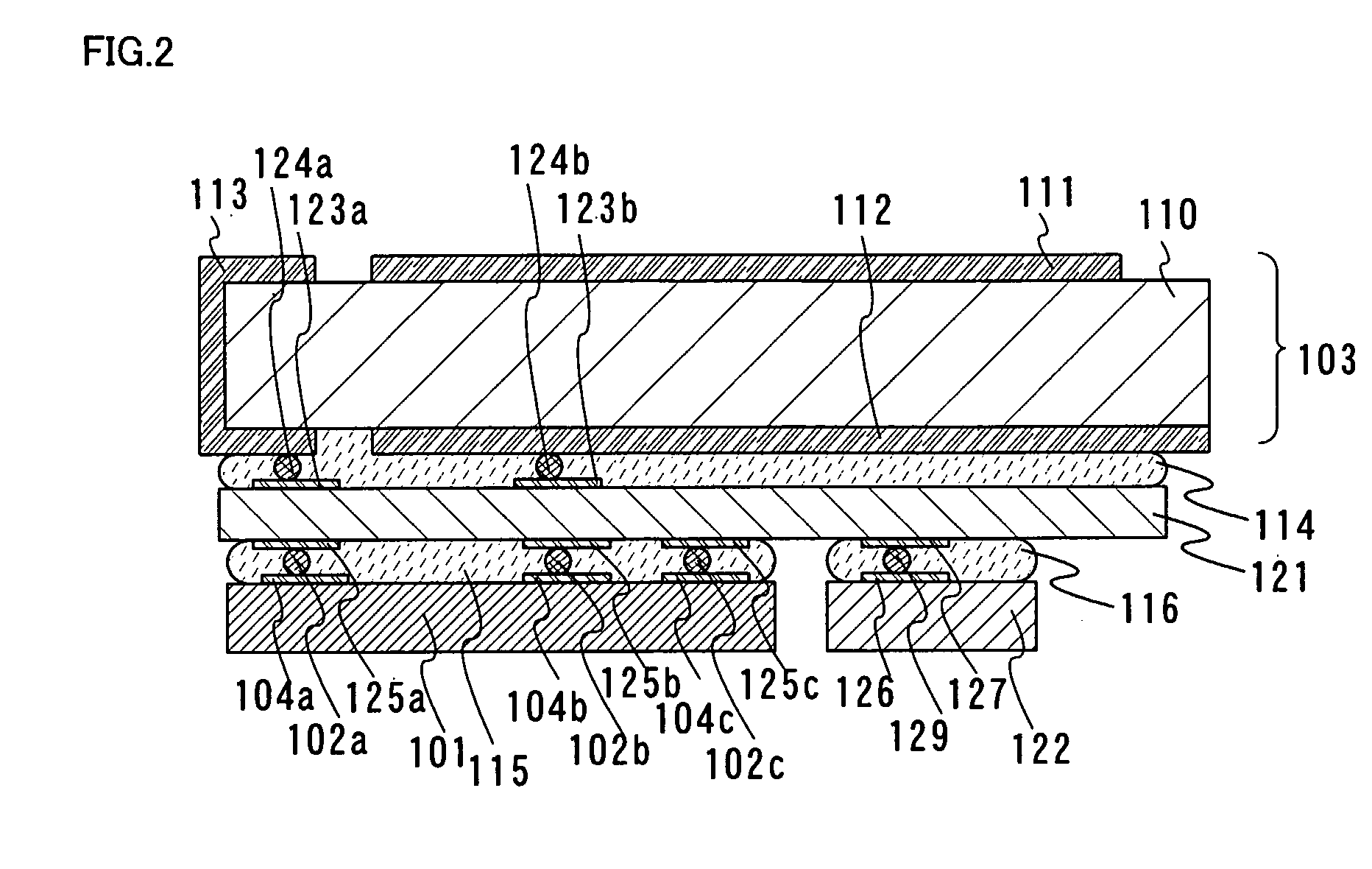
[0077]A description is made on one embodiment mode of a wireless chip of the present invention referring to FIG. 2. FIG. 2 is a cross-sectional diagram of a wireless chip. In the present embodiment mode, description is made on a structure of a wireless chip including a chip having a field-effect transistor, a patch antenna, and a sensor device.

[0078]The chip 101 having a field-effect transistor is mounted on a wiring substrate 121, in the wireless chip of the present embodiment mode. Specifically, connection terminals 104a to 104c formed over the surface of the chip 101 having a field-effect transistor and connection terminals 125a to 125c formed over the wiring substrate 121 are connected by conductive layers 102a to 102c, respectively.

[0079]A sensor device 122 is mounted over the wiring substrate 121. Specifically, a connection terminal 126 formed over the surface of the sensor device 122 and a connection terminal 127 formed over the wiring substrate 121 are connected by a conduct...

embodiment mode 3

[0095]A description is made on one embodiment mode of a wireless chip of the present invention referring to FIG. 3. FIG. 3 is a cross-sectional diagram of the wireless chip.

[0096]The wireless chip of the present embodiment mode is one in which a battery is added to the wireless chip shown in Embodiment Mode 1. Specifically, the connection terminals 104a to 104c formed over the surface of the chip 101 having a field-effect transistor and the connection terminals 125a to 125c formed over the wiring substrate 121 are connected by the conductive layers 102a to 102c, respectively.

[0097]A battery 141 is mounted over the wiring substrate 121. Specifically, a connection terminal 142 formed over the surface of the battery 141 and a connection terminal 143 formed over the wiring substrate 121 are connected by a conductive layer 144.

[0098]Note that the connection terminals 125a to 125c formed over the wiring substrate 121 and the connection terminal 143 are connected by the conductive layer su...


PUM


Abstract

It is an object to provide a wireless chip which can increase a mechanical strength, and a wireless chip with a high durability. A wireless chip includes a transistor including a field-effect transistor, an antenna including a dielectric layer sandwiched between conductive layers, and a conductive layer connecting the chip and the antenna. Further, a wireless chip includes a transistor including a field-effect transistor, an antenna including a dielectric layer sandwiched between conductive layers, a sensor device, a conductive layer connecting the chip and the antenna, and a conductive layer connecting the chip and the sensor device. Moreover, a wireless chip includes a transistor including a field-effect transistor, an antenna including a dielectric layer sandwiched between conductive layers, a battery, a conductive layer connecting the chip and the antenna, and a conductive layer connecting the chip and the battery.

Description

TECHNICAL FIELD[0001]The present invention relates to a wireless chip which can communicate data by wireless communication and an electronic device having a wireless chip.BACKGROUND ART[0002]In recent years, development of a wireless chip including a plurality of circuits and an antenna is advanced. Such a wireless chip is called as an ID tag, an IC tag, an IC chip, an RF (Radio Frequency) tag, a wireless tag, an electronic tag, and an RFID (Radio Frequency Identification) tag, and has already been introduced into some markets.[0003]Many of these wireless chips which are put into practical use at present, include a circuit (referred to as an IC (Integrated Circuit) chip) with the use of a semiconductor substrate such as a silicon and an antenna. The antenna is formed by a technique such as a printing method, a method of etching a conductive thin film, and a plating method (for example, refer to the Patent Document 1).[Patent Document 1] Japanese Patent Laid-Open No. Hei9-1970DISCLOS...

Claims


Application Information

Patent Timeline
Patent Type & Authority Applications(United States)
IPC IPC(8): H01Q23/00H01Q1/38
CPCH01Q1/2208H01Q9/0407H01Q1/243H01L2223/6677H01L2224/0401H01L2224/16227H01L2224/32225H01L2224/73204H01L2924/15311H01L2224/16225H01L2924/00
Inventor SUZUKI, YUKIEARAI, YASUYUKIYAMAZAKI, SHUNPEI
Owner SEMICON ENERGY LAB CO LTD
Why Eureka
Try Eureka