

Method of manufacturing a semiconductor device
a manufacturing method and semiconductor technology, applied in semiconductor devices, semiconductor/solid-state device details, electrical devices, etc., can solve the problems of failure to blow fuse, yield and reliability, and invite fuse corrosion, so as to improve yield and reliability, and control the etching of dielectric films.
- Summary
- Abstract
- Description
- Claims
- Application Information
AI Technical Summary
Benefits of technology
Problems solved by technology
Method used
Image

Examples
first embodiment
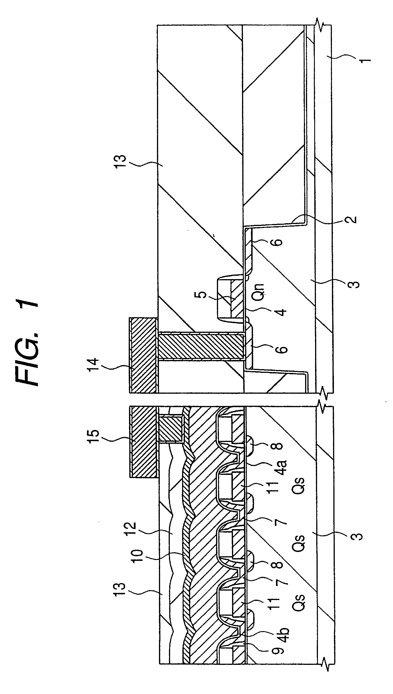
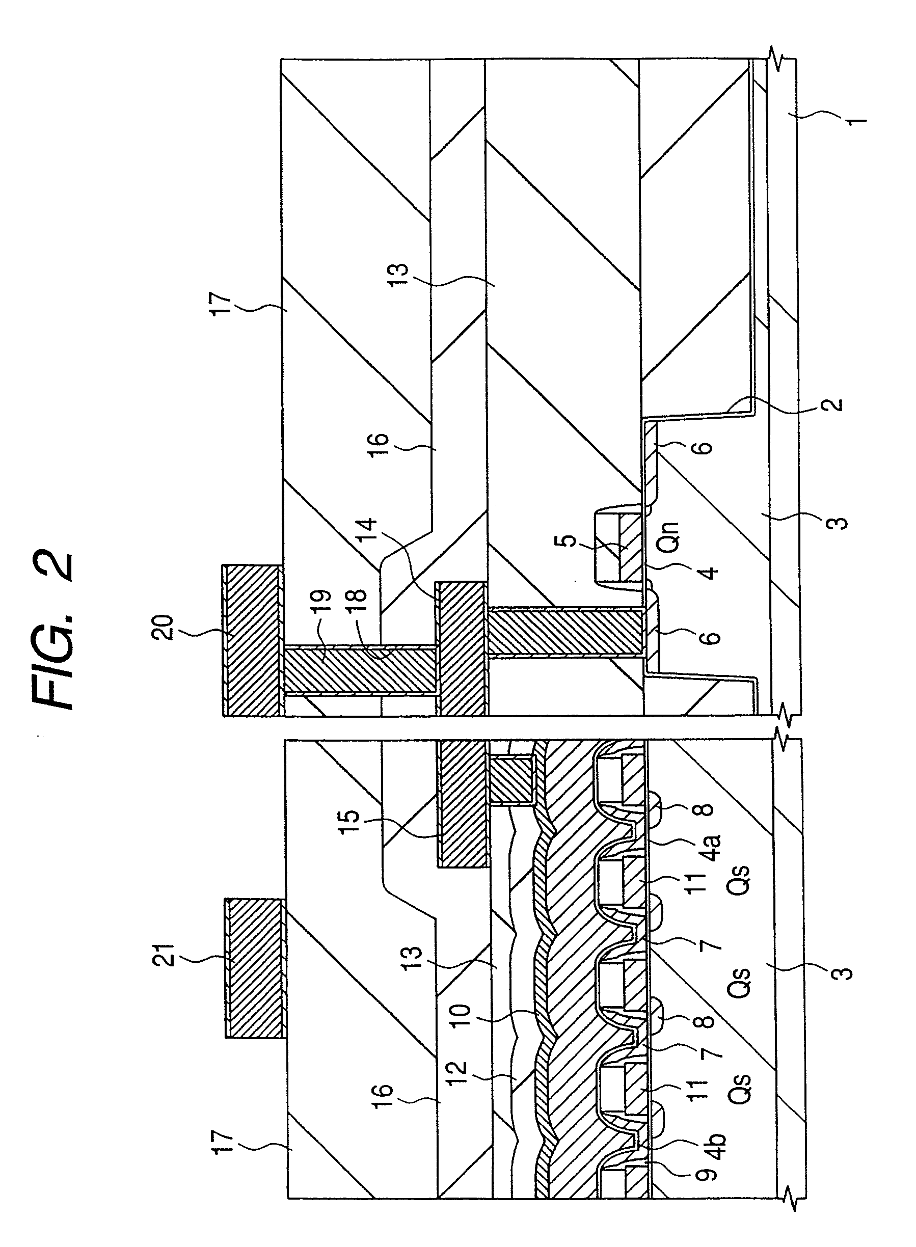
[0042]A method of manufacturing a semiconductor device will be sequentially described, step by step with reference to FIGS. 1 to 11. In the method, an opening is formed in a dielectric film arranged over a fuse. The left-hand parts in individual sectional views each represent a fuse-forming region and the right-hand parts thereof represent a bonding pad (hereinafter referred to as a “pad”) forming region.
[0043]With reference to FIG. 1, a device isolation trench 2, a p-type well 3, memory cells Qs serving as a flash memory, and an n-channel MISFET Qn serving as a peripheral circuit, for example, are initially formed on a semiconductor substrate (hereinafter referred to as a “substrate”) 1 according to conventional manufacturing processes. The substrate 1 comprises, for example, a p-type single-crystal silicon. Next, dielectric films, such as silicon oxide films 12 and 13, are formed over the memory cells Qs and the n-channel MISFET Qn by chemical vapor deposition (CVD). First-level w...
second embodiment
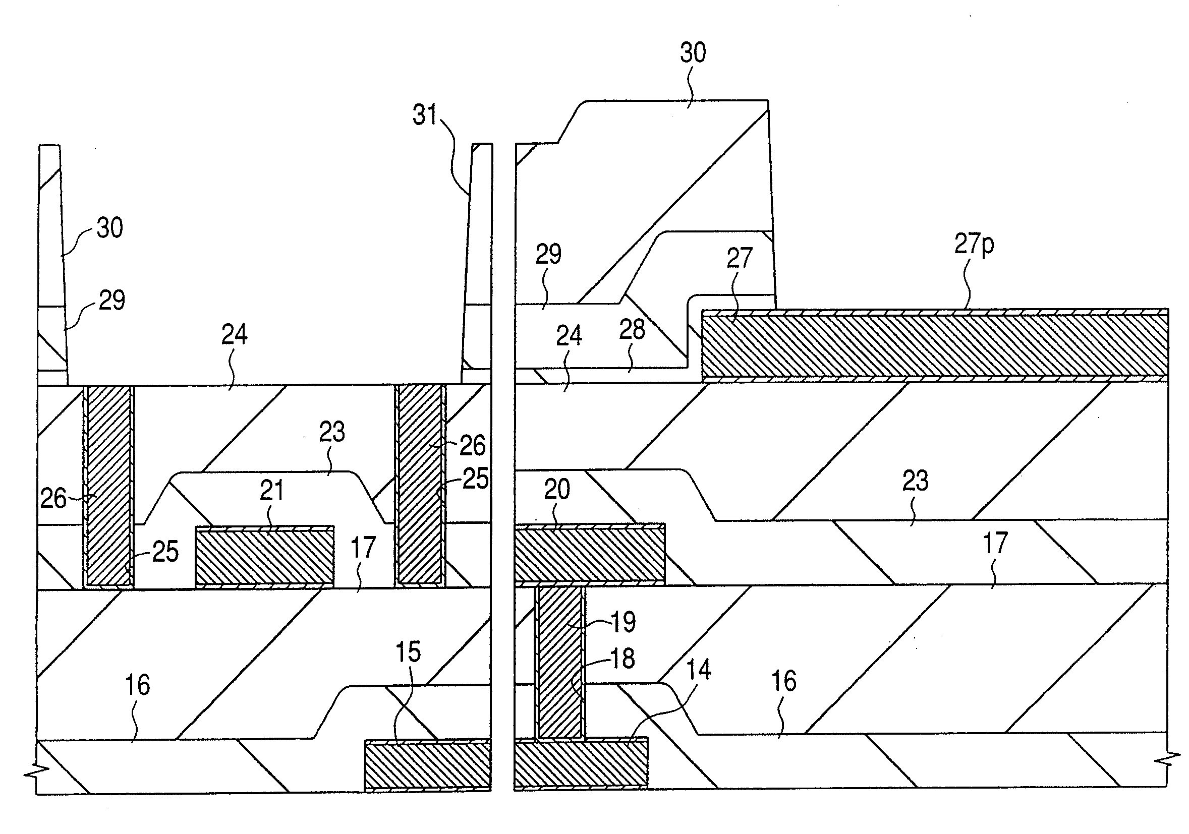
[0062]Another method of manufacturing a semiconductor device will be described with reference to FIGS. 12 to 16. In this method, a through hole is formed in a dielectric film over wirings.
[0063]Initially, as seen with reference to FIG. 12, a device isolation trench 2, a p-type well 3, an n-channel MISFET Qn and other components are formed on a substrate 1 according to conventional manufacturing procedures. A dielectric film, such as a silicon oxide film 13, is formed on the n-channel MISFET Qn by CVD, a surface of the silicon oxide film 13 is planarized by chemical mechanical polishing, and an SRO film 28 is formed over the silicon oxide film 13. The thickness of the SRO film 28 is set, for example, at about 70 nm. The SRO film 28 has the same configuration and is formed by the same manufacturing procedure as used in the First Embodiment.
[0064]With reference to FIG. 13, the SRO film 28 and the silicon oxide film 13 are dry-etched to form a contact hole 40, a metal plug 41 is charged...
PUM
 Abstract
Description
Claims
Application Information