Device for controlling exposure of reservoir contents to surroundings
a reservoir and reservoir technology, applied in the direction of micromachined delivery, laboratory glassware, medical preparations, etc., can solve the problems of drug delivery, patients often forget, are unwilling, or are unable to take their medication, and the selection of a proper drug delivery method is problemati
- Summary
- Abstract
- Description
- Claims
- Application Information
AI Technical Summary
Benefits of technology
Problems solved by technology
Method used
Image


Examples
example 1
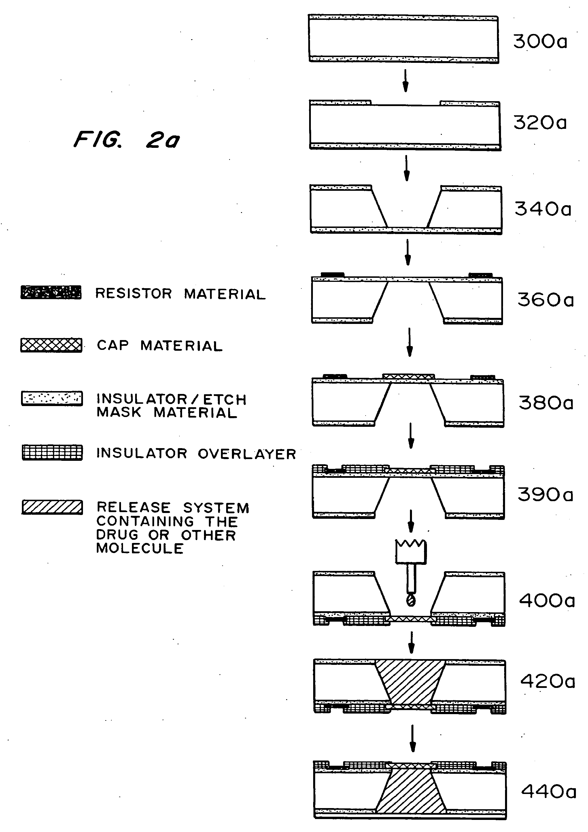
Fabrication of an Active Release Microchip Having Resistors Near the Reservoir Cap
[0089]1) Obtain double side polished, prime grade, (100) oriented silicon wafers, i.e., substrates.
[0090]Wafer thickness=approximately 295-310 μm
2) Deposit approximately 1600-1900 Å of low stress (10:1, silicon rich) silicon nitride on both sides of the wafers in an SVG / Thermco 7000 Series vertical tube reactor (VTR), 300a / 300b / 300c / 300d.
[0091]Gas Flows: Ammonia (NH3)=24 sccm[0092]Dichlorosilane (SiH2Cl2)=253 sccm
[0093]Chamber Pressure=268 mtorr; Temperature=780° C.
[0094]Deposition Rate=approximately 30 Å / min.
3) Pattern positive photoresist (PR) as squares (approximately 500 μm by 500 μm) serving as the large reservoir openings on one side of the wafers having low stress silicon nitride deposited on them.
[0095]Hexamethyldisilazane deposition on both sides of the wafer[0096](“HMDS vapor prime”) in vacuum oven approximately 30 min. at 150° C.
[0097]Photoresist (PR) Type—OCG825-20
[0098]PR Spin Speed and T...
example 2
Fabrication of an Active Release Microchip Having Resistors in the Reservoirs
[0179]1) thru 7) The steps for producing a first wafer containing nitride membrane covered reservoirs are the same as in Example 1.
8) Pattern image reversal PR on a second wafer 370a / 370b (e.g., silicon wafer or other substrate such as glass) for subsequent platinum liftoff process.
[0180]HMDS vapor prime in vacuum oven: approximately 30 min. at 150° C.
[0181]Photoresist Type (PR)—AZ 5214 E
[0182]PR Spin Speed and Times (for a Solitec Inc. Model 5110 spinner)[0183]6 sec. at 500 rpm (coat); 6 sec. at 750 rpm (spread); and[0184]30 sec. at 4000 rpm (spin)
[0185]Prebake (in Blue M Model DDC-146C oven): 30 min. at 90° C.
[0186]Ultra-violet (UV) exposure for each wafer in the contact aligner
[0187](Karl Suss Model MA4) with patterned mask[0188]40 sec. at wavelength=320 nm
[0189]Bake for 90 sec. on a metal plate in an oven at 120° C. (Blue M Model DDC-146C)
[0190]UV flood exposure for each wafer in the contact aligner (Ka...
example 3
Fabrication of a Passive Release Microchip
[0207]1) Obtain double side polished, prime grade, (100) oriented silicon wafers for devices having reservoirs extending completely through the wafer or single side polished, prime grade, (100) oriented silicon wafers for devices having reservoirs that do not extend completely through the wafer.[0208]Wafer thickness=approximately 295-310 μm for devices with reservoirs extending completely through the wafer (devices that do not have reservoirs extending all the way through the wafer can be of any desired thickness)
2) Deposit approximately 1600-1900 Å of low stress (10:1, silicon rich) silicon nitride on both sides of the wafers in an SVG / Thermco 7000 Series vertical tube reactor (VTR) 30.
[0209]Gas Flows: Ammonia (NH3)=24 sccm[0210]Dichlorosilane (SiH2Cl2)=253 sccm
[0211]Chamber Pressure=268 mtorr; Temperature=780° C.
[0212]Deposition Rate=approximately 30 Å / min.
3) Pattern positive PR as squares (approximately 500 μm by 500 μm for devices with r...
PUM
 Abstract
Description
Claims
Application Information
 - R&D
- Intellectual Property
- Life Sciences
- Materials
- Tech Scout
- Unparalleled Data Quality
- Higher Quality Content
- 60% Fewer Hallucinations
Browse by: Latest US Patents, China's latest patents, Technical Efficacy Thesaurus, Application Domain, Technology Topic, Popular Technical Reports.
© 2025 PatSnap. All rights reserved.Legal|Privacy policy|Modern Slavery Act Transparency Statement|Sitemap|About US| Contact US: help@patsnap.com