Mother substrate of organic light emitting display devices and method of aging the same

a technology of organic light-emitting display devices and mother substrates, applied in the field of display devices, can solve the problems of increasing or aggravated voltage drop (ir drop) in sheet wires, driving problems or bright defects in some panels, and achieve the effect of improving the efficiency of the aging process

Inactive Publication Date: 2009-11-12
SAMSUNG DISPLAY CO LTD
View PDF10 Cites 23 Cited by
  • Summary
  • Abstract
  • Description
  • Claims
  • Application Information

AI Technical Summary

Benefits of technology

[0017]Accordingly, the present invention is designed to address drawbacks of the prior art. In one embodiment, the present invention provides a mother substrate of an organic light emitting display device capable of effectively aging a plurality of organic light emitting display panels sheet by sheet by shortening the aging time while preventing driving problems and bright defects in the panels.
[0029]Also, the mother substrate of an organic light emitting display device according to the present invention may be useful to reduce the aging time and also to prevent the driving problems and bright defects in the panels by applying different voltage levels for a reference power voltage (for example, a high level gate voltage (VGH)) supplied to the panels in consideration of the voltage drop of a pixel power source (for example, a first pixel power source (ELVDD)) supplied through sheet wires.
[0031]Therefore, the mother substrate of an organic light emitting display device according to the present invention may be used to improve the efficiency of the aging process.

Problems solved by technology

However, the inspection process can be inefficient since the inspection needs to be separately carried out on each of the panels.
However, the increase in current value results in increased or aggravated voltage drop (IR drop) in sheet wires that supply driver power sources and / or drive signals to each of the panels.
This may cause driving problems or bright defects in some panels when aging is carried out sheet by sheet.
In particular, when the voltage drop of the first pixel power source (ELVDD) is severe, the voltage difference of ELVDD from the first reference power voltage (VGH) of a scan driver is different in every panel, which results in the driving problems and / or bright defects in the panels.

Method used


Image

  • Mother substrate of organic light emitting display devices and method of aging the same
  • Mother substrate of organic light emitting display devices and method of aging the same
  • Mother substrate of organic light emitting display devices and method of aging the same

Examples


Embodiment Construction

[0038]Hereinafter, certain exemplary embodiments according to the present invention will be described with reference to the accompanying drawings. Here, when a first element is described as being coupled to a second element, the first element may be directly coupled to the second element or may be indirectly coupled to the second element via a third element. Further, some of the elements that are not essential to a complete understanding of the invention are omitted for clarity. Also, like reference numerals refer to like elements throughout.

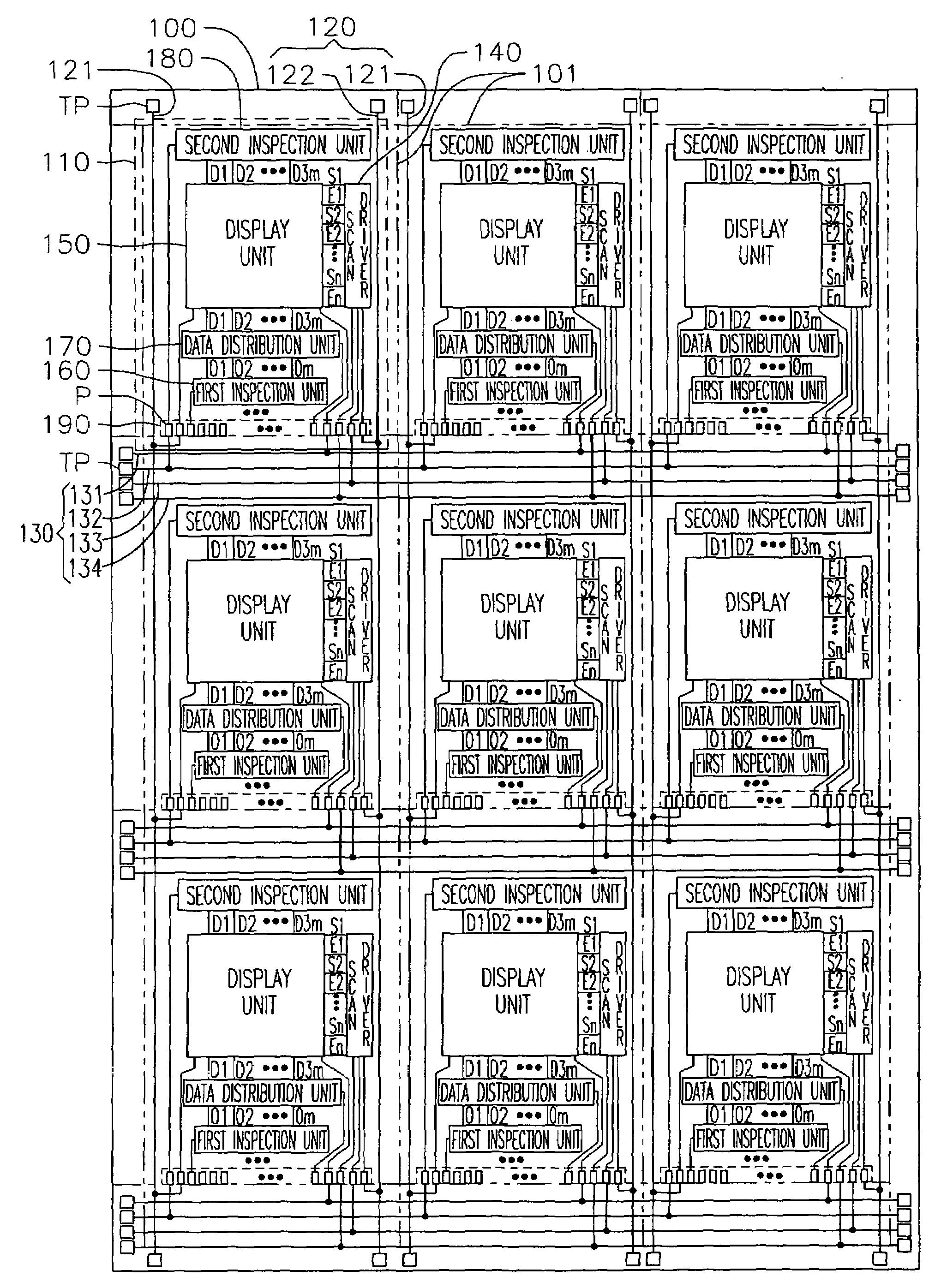
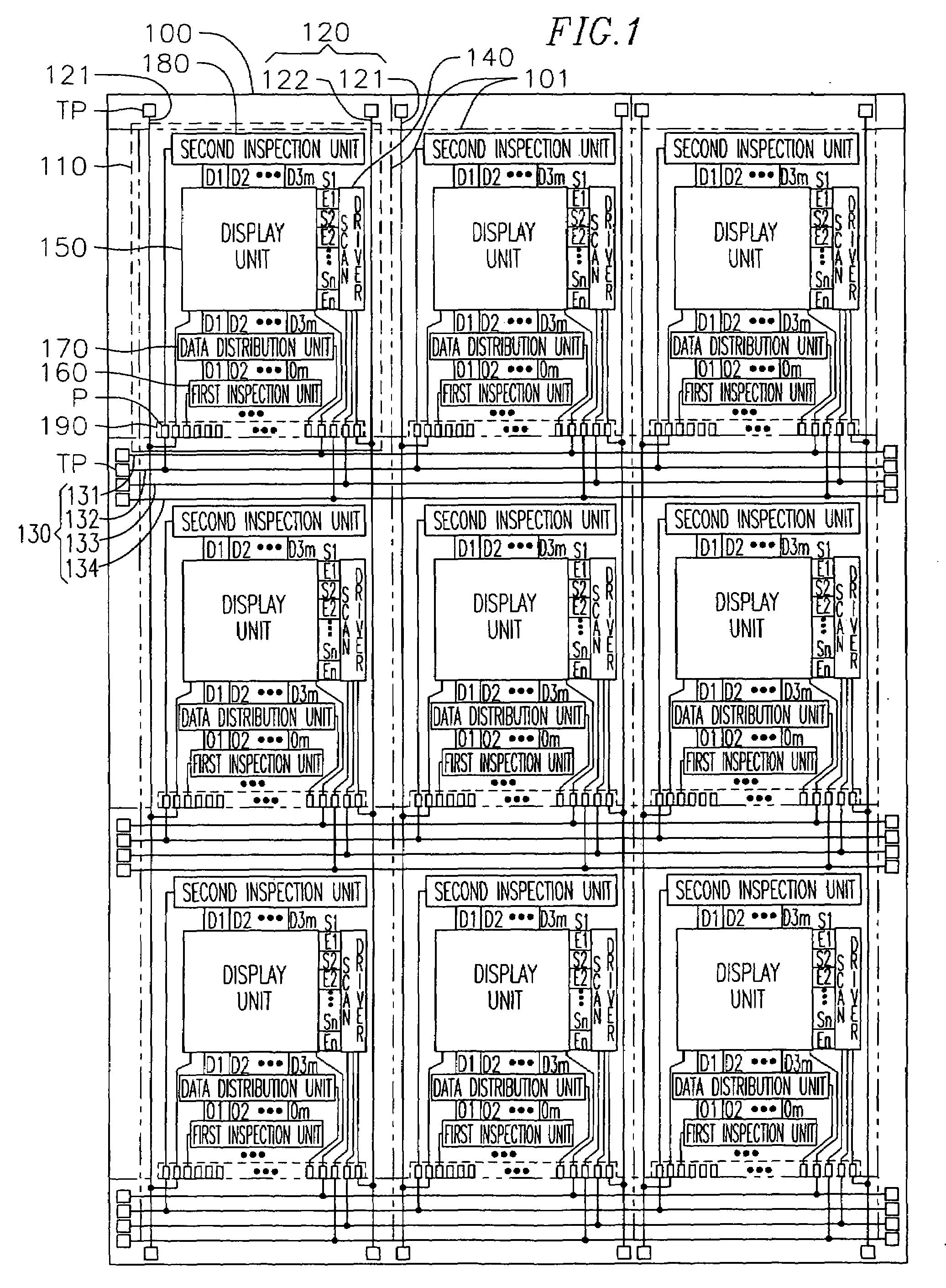
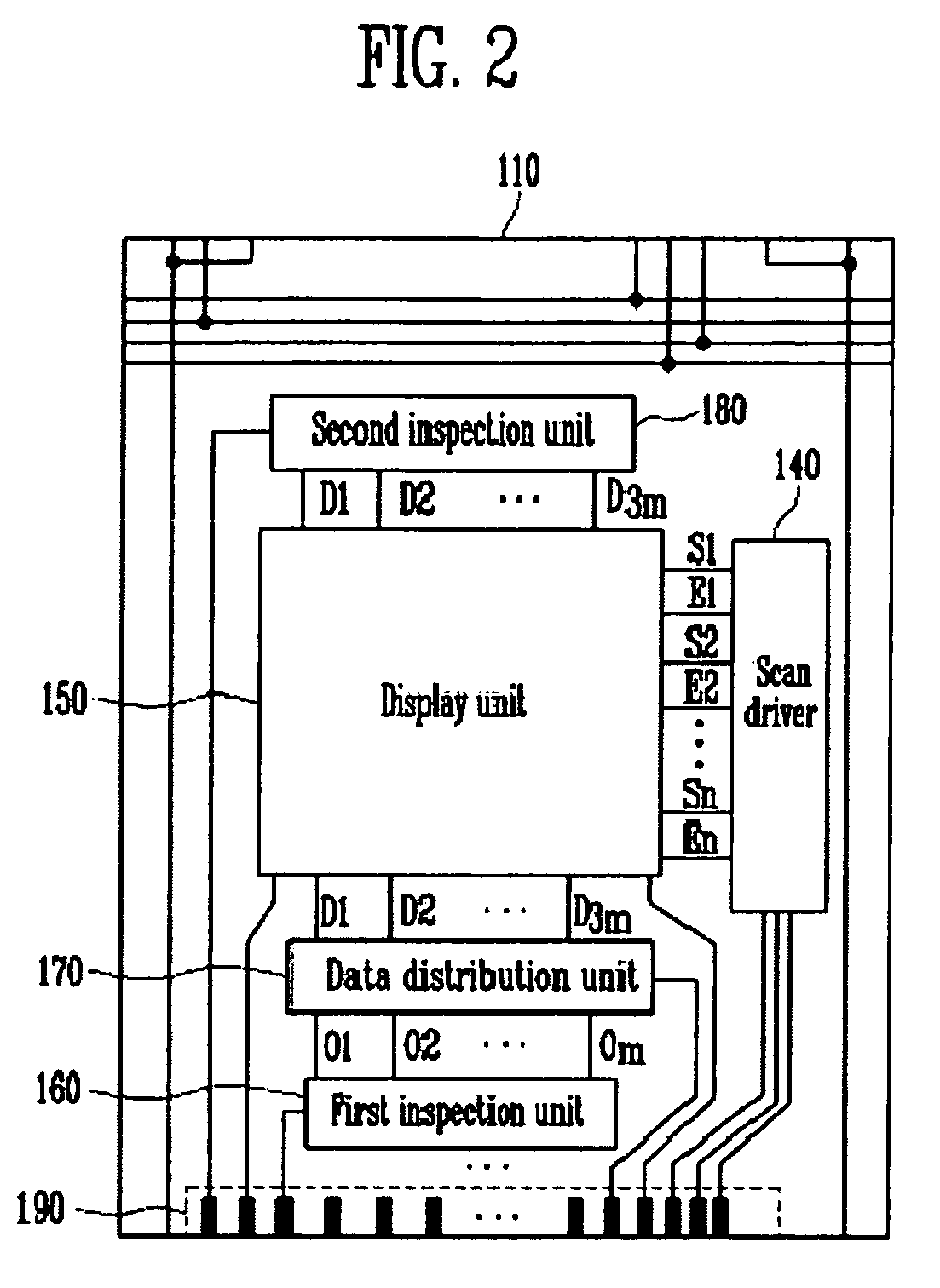
[0039]FIG. 1 is a plan view showing a mother substrate of an organic light emitting display device according to one exemplary embodiment of the present invention. FIG. 2 is a plan view showing an organic light emitting display panel that has been scribed from the mother substrate as shown in FIG. 1.

[0040]Referring to FIGS. 1 and 2, the mother substrate 100 of an organic light emitting display device according to one exemplary embodiment of prese...


PUM


Abstract

A mother substrate of an organic light emitting display device capable of effectively aging a plurality of organic light emitting display panels by sheet unit without scribing the panels is provided. In one embodiment, the invention relates to a substrate of an organic light emitting display device, including a plurality of organic light emitting display panels, a plurality of first wires configured to supply a pixel power source to the panels in a first direction, and a plurality of second wires configured to supply a reference power voltage to the panels in a second direction crossing the first direction, wherein voltage levels of the reference power voltage are set to different voltage levels relative to a position of panels on the substrate.

Description

CROSS-REFERENCE TO RELATED APPLICATION[0001]This application claims priority to and the benefit of Korean Patent Application No. 10-2008-0042211, filed on May 7, 2008, in the Korean Intellectual Property Office, the entire content of which is incorporated herein by reference.BACKGROUND OF THE INVENTION[0002]1. Field of the Invention[0003]The present invention relates to display devices, and more particularly to a mother substrate of an organic light emitting display device and a method of aging the same.[0004]2. Description of Related Art[0005]In general, a plurality of organic light emitting display panels are formed with one mother substrate, scribed and separated into respective panels. That is to say, in order to more effectively manufacture a large number of organic light emitting display devices, a so-called sheet-unit manufacturing method has been developed, which includes: forming panels of a plurality of organic light emitting display devices with one mother substrate and s...

Claims


Application Information

Patent Timeline
Patent Type & Authority Applications(United States)
IPC IPC(8): G09G5/00G09G3/30
CPCG09G3/006G09G3/3233G09G2300/0819G09G2320/043G09G2300/0861G09G2310/0218G09G2300/0842H10K59/10
Inventor KA, JI-HYUN
Owner SAMSUNG DISPLAY CO LTD
Why Eureka
Try Eureka