

Probe device and method of regulating contact pressure between object to be inspected and probe
a technology of a probe and a probe body, which is applied in the direction of measurement devices, semiconductor/solid-state device testing/measurement, instruments, etc., can solve the problems of inability to obtain proper contact pressure, and insufficient reliability of inspection results, so as to improve the reliability of inspection of electrical characteristics of target objects.
- Summary
- Abstract
- Description
- Claims
- Application Information
AI Technical Summary
Benefits of technology
Problems solved by technology
Method used
Image

Examples
Embodiment Construction
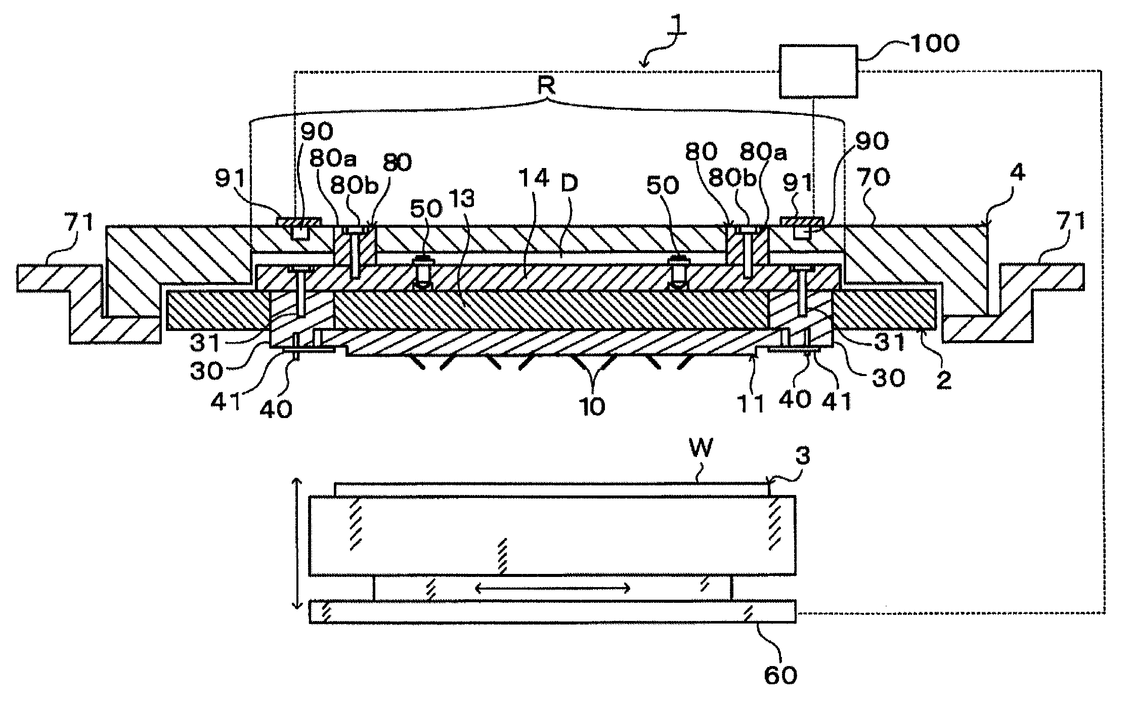
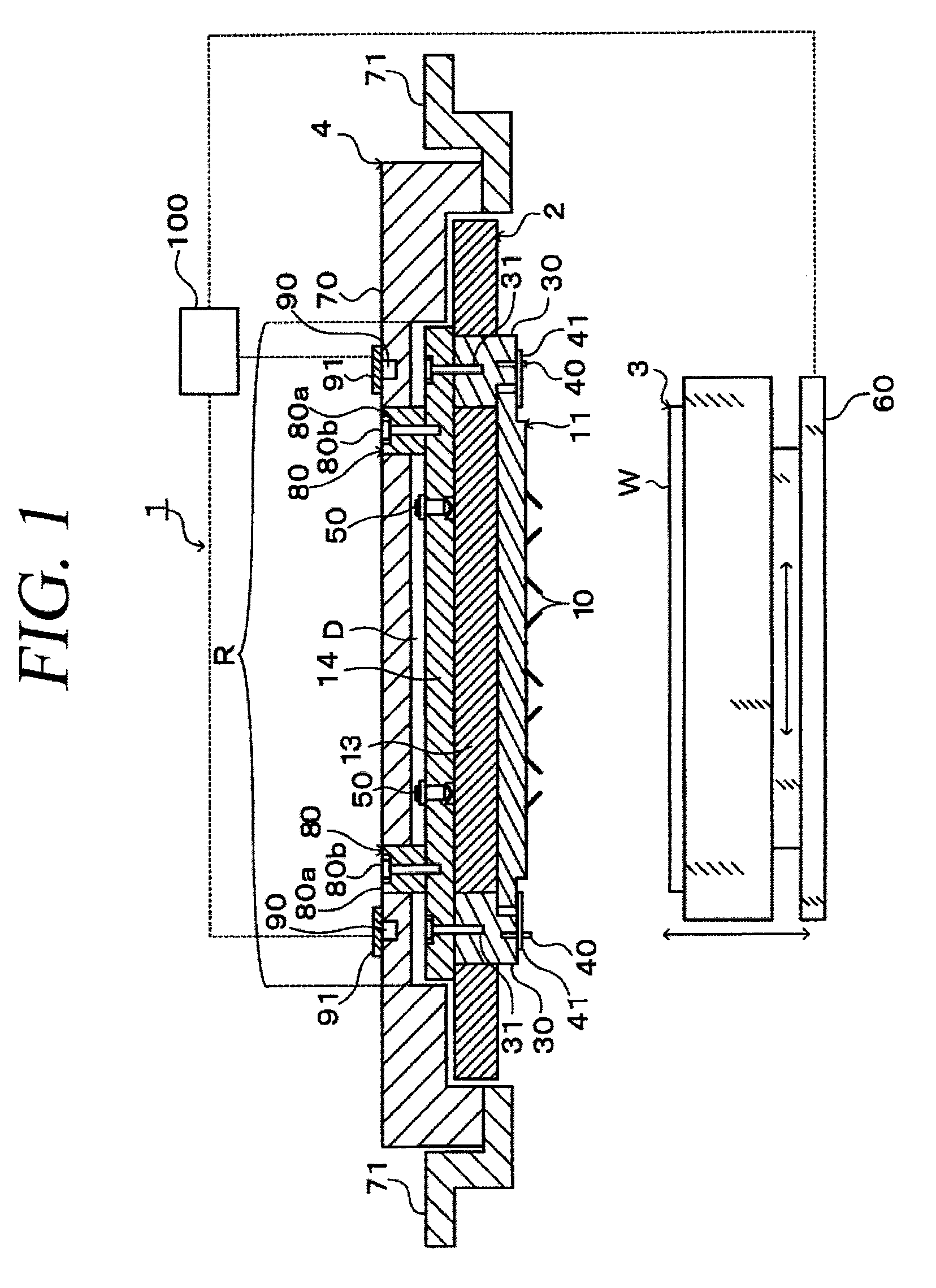
[0037]Hereinafter, an embodiment of the present invention will be described. FIG. 1 is a longitudinal cross sectional view showing a schematic internal configuration of a probe device 1 in accordance with the embodiment of the present invention.
[0038]The probe device 1 includes, for example, a probe card 2; a mounting table 3 for mounting thereon a wafer W which is a target object to be inspected; and a card holder 4 for holding the probe card 2.
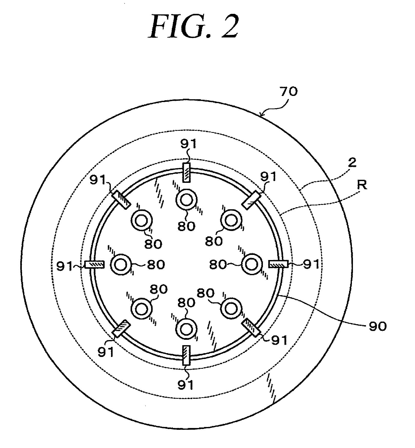
[0039]The probe card 2 is formed in, for example, a substantially disk-like shape as a whole. The probe card 2 includes a contactor 11 sustaining a plurality of probes 10 thereon; a printed wiring board 13 electrically connected with the contactor 11; and a reinforcement member 14 for reinforcing the printed wiring board 13.
[0040]The contactor 11 is formed in, for example, a substantially rectangular plate shape, and is disposed on a lower side of the probe card 2 to face the mounting table 3. The plurality of probes 10 are connected to and ...
PUM
 Abstract
Description
Claims
Application Information