Substrate processing apparatus, control method for the apparatus, and program for implementing the method

a processing apparatus and control method technology, applied in the field of substrate processing apparatus, can solve the problems of reduced reliability, reduced reliability, and increased user burden, and achieve the effect of reducing user burden and improving reliability

Active Publication Date: 2008-09-18
TOKYO ELECTRON LTD
View PDF5 Cites 4 Cited by
  • Summary
  • Abstract
  • Description
  • Claims
  • Application Information

AI Technical Summary

Benefits of technology

[0017]It is an object of the present invention to provide a substrate processing apparatus, a control method for the apparatus, and a program for implementing the method, according to which inspection of various devices in the substrate processing apparatus can be carried out with improved reliability, while reducing the burden on a user.
[0030]According to the present invention, the housing state relating to the arrangement of the inspection substrates in the container is stored as setup information over a period spanning before and after replacement of inspection substrates in the container. As a result, the necessity for a user to newly input / set setup information to the substrate processing apparatus every time inspection substrate replacement is carried out is eliminated, and moreover mismatches between the inputted / set setup information and the actual housing state of inspection substrates in the container due to input mistakes by the user can be prevented. The reliability of inspection of the various devices in the substrate processing apparatus can thus be improved, while reducing the burden on the user.
[0032]According to the present invention, another set of setup information obtained by carrying out editing based on the selected desired set of setup information may be stored. As a result, the user can input / set a new set of setup information based on the desired set of setup information selected by the user, and hence the efficiency of inputting / setting of the setup information by the user can be further improved, and moreover input mistakes by the user can be reduced as much as possible, and hence the reliability of inspection of the various devices in the substrate processing apparatus can be further improved.

Problems solved by technology

Consequently, if the substrate processing apparatus continues to use the setup information for the dummy wafers in the FOUP 500 as it is, then confusion may arise.
However, the lifetime of a dummy wafer is approximately 1 to 2 weeks during mass production of semiconductor wafers, and in particular is only approximately 2 to 3 days in the case of inspection of processing in a corrosive system.
Under such a situation, there is a problem that if the setup information for the dummy wafers in the FOUP 500 is deleted from the HDDD or the like of the substrate processing apparatus, then the user must newly input / set setup information to the substrate processing apparatus every time dummy wafer replacement is carried out and hence there is a considerable burden on the user.
Furthermore, in mass production of semiconductor wafers, during dummy wafer replacement, it is mostly the case that the dummy wafer inserted into a particular slot is for the same type of inspection as the dummy wafer that was in that slot before the replacement, and hence there is little fear of the confusion described above arising; if anything, there is a problem that during inputting / setting of setup information by the user, mismatches between the inputted / set setup information and the actual housing state of the dummy wafers in the FOUP 500 may arise due to input mistakes, resulting in it not being possible to carry out inspection of the various devices in the substrate processing apparatus smoothly, and hence there being a drop in reliability.

Method used


Image

  • Substrate processing apparatus, control method for the apparatus, and program for implementing the method
  • Substrate processing apparatus, control method for the apparatus, and program for implementing the method
  • Substrate processing apparatus, control method for the apparatus, and program for implementing the method

Examples


Embodiment Construction

[0041]The present invention will now be described in detail with reference to the drawings showing preferred embodiments thereof.

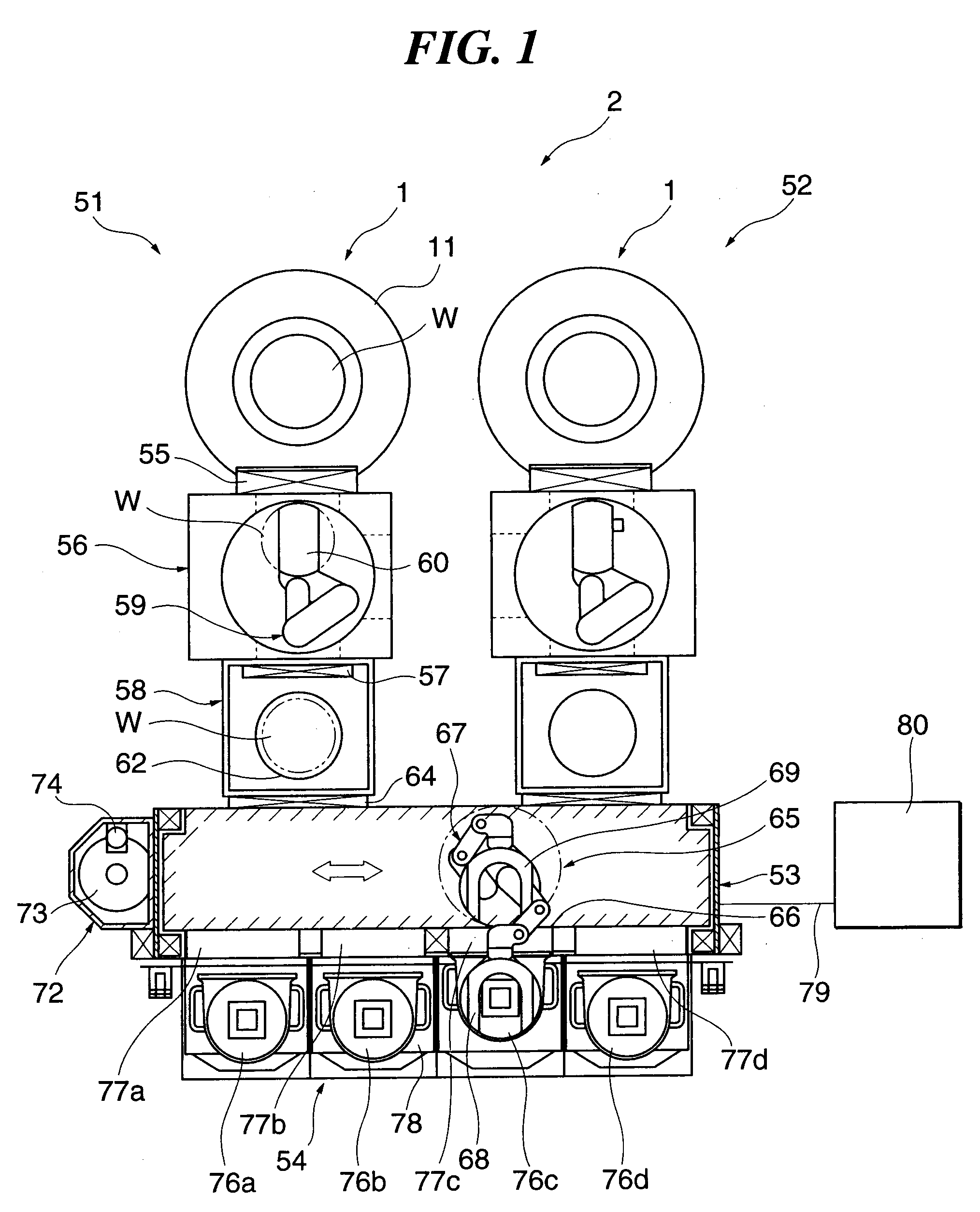
[0042]FIG. 1 is a plan view schematically showing the construction of a substrate processing apparatus according to an embodiment of the present invention.

[0043]In FIG. 1, a plasma processing system 2, as the substrate processing apparatus according to the present embodiment, has a first processing unit 51 and a second processing unit 52 in which are carried out etching on semiconductor wafers W, a substrate transferring in / out stage 53, FOUP platforms 54 having FOUPs mounted thereon, and a control unit 80 that controls the operation of the plasma processing system 2.

[0044]The first processing unit 51 is comprised of a plasma processing apparatus 1 having a processing chamber 11 in which etching is carried out on the semiconductor wafers W, a transfer chamber 56 that is connected to the processing chamber 11 of the plasma processing apparatus 1 via a gate ...


PUM

PropertyMeasurementUnit
lifetimeaaaaaaaaaa
diameteraaaaaaaaaa
box shapeaaaaaaaaaa

Abstract

A substrate processing apparatus, according to which inspection of various devices in the substrate processing apparatus can be carried out with improved reliability, while reducing the burden on a user. A processing chamber processes semiconductor wafers therein. A transfer chamber transfers the semiconductor wafers. A FOUP (front opening unified pod) houses a plurality of dummy wafers for inspection of the processing chamber or the transfer chamber. A CPU causes an HDD (hard disk drive) to store a housing state relating to the arrangement of the dummy wafers in the FOUP before replacement of dummy wafers in the FOUP and that after the replacement as dummy wafer setup information.

Description

CROSS REFERENCE[0001]This application is a division of and is based upon and claims the benefit of priority under 35 U.S.C. §120 for U.S. Ser. No. 10 / 984,982, filed Nov. 10, 2004, and claims the benefit of priority under 35 U.S.C. §119 from Japanese Patent Application No. 2003-383008, filed Nov. 12, 2003.BACKGROUND OF THE INVENTION[0002]1. Field of the Invention[0003]The present invention relates to a substrate processing apparatus that carries out processing on substrates as objects to be processed, a control method for the apparatus, and a program for implementing the method, and in particular relates to a substrate processing apparatus that carries out processing on dummy wafers, a control method for the apparatus, and a program for implementing the method.[0004]2. Description of the Related Art[0005]Conventionally, in the manufacture of substrates (objects to be processed) for flat panel displays, semiconductor wafers and so on, substrate processing apparatuses comprised of at l...

Claims


Application Information

Patent Timeline
Patent Type & Authority Applications(United States)
IPC IPC(8): H01L21/02G06F19/00H01L21/677H01L21/00
CPCH01L21/67294H01L21/67276Y10S414/135
Inventor SHIMIZU, NORIAKINUMAKURA, MASAHIRO
Owner TOKYO ELECTRON LTD
Why Eureka
Try Eureka