Method for forming a concavo-convex textured structure on a housing of an electronic device and related structure

a technology of concave and convex, which is applied in the direction of electrical programme control, instruments, program control, etc., can solve the problems that the method may only be able to form a simple the concave-convex textured structure on the workpiece formed by the chemical etching process cannot have a smooth outline, and the related manufacturing process is strenuous and time-consuming

Inactive Publication Date: 2011-01-13
WISTRON CORP
View PDF14 Cites 6 Cited by
  • Summary
  • Abstract
  • Description
  • Claims
  • Application Information

AI Technical Summary

Problems solved by technology

However, the said methods may only be capable of forming a simple textured structure on the workpiece since the chemical solution used in the chemical etching process can just etch the surface of the workpiece vertically and shallowly.
Thus, related manufacturing processes are strenuous and time-consuming.
Furthermore, because the chemical solution used in the chemical etching process can just etch the surface of the workpiece vertically, a concavo-convex textured structure on a workpiece formed by the chemical etching process cannot have a smooth outline.
Thus, if the workpiece is utilized as a mold for molding an ink layer of a film in an IMR (In Mold Roller) process, the film may be incapable of attaching to the workpiece closely and completely due to the unsmooth structure on the workpiece.
In such a manner, the film may be broken during the IMR process.

Method used


Image

  • Method for forming a concavo-convex textured structure on a housing of an electronic device and related structure
  • Method for forming a concavo-convex textured structure on a housing of an electronic device and related structure
  • Method for forming a concavo-convex textured structure on a housing of an electronic device and related structure

Examples


Embodiment Construction

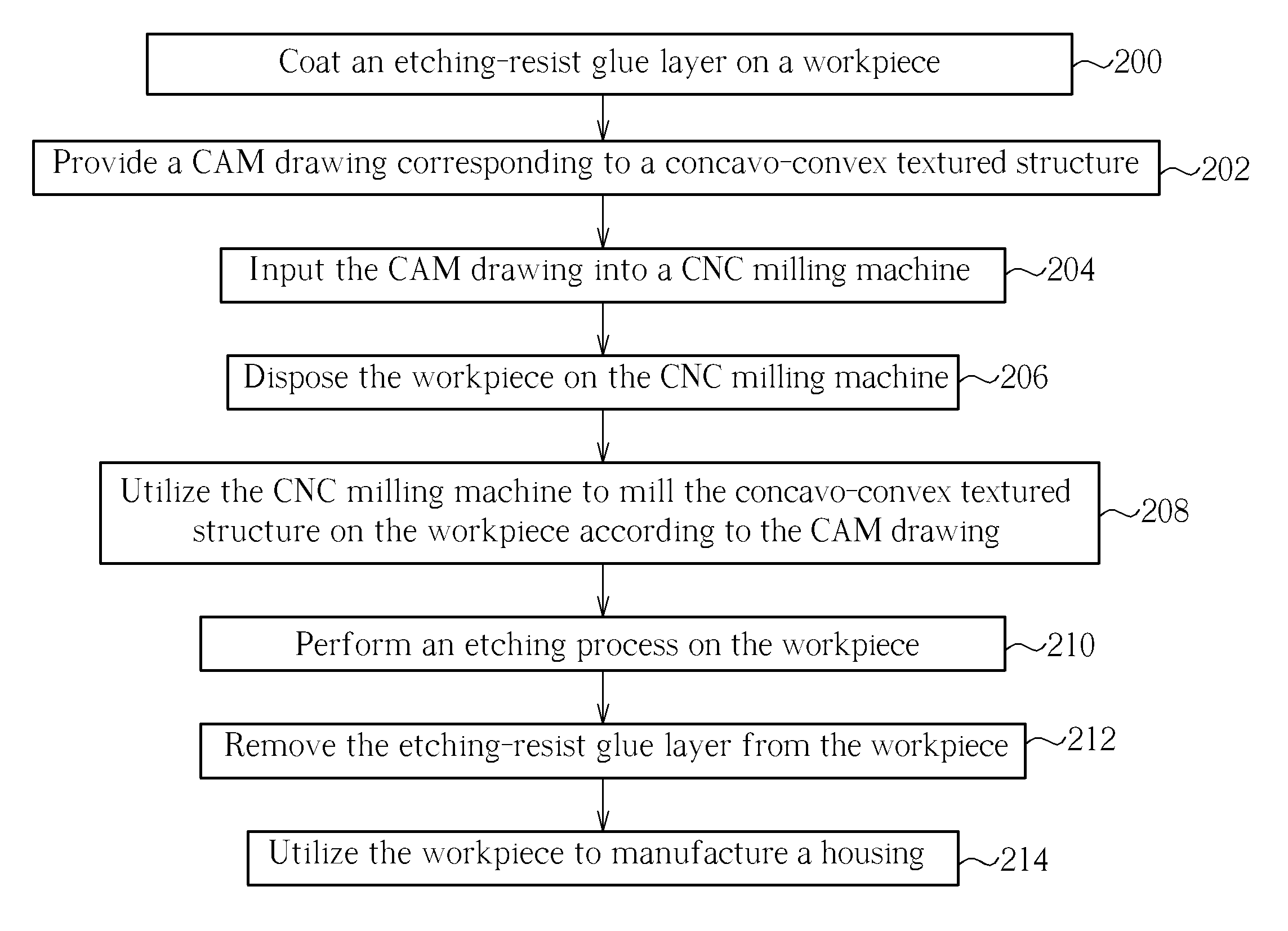
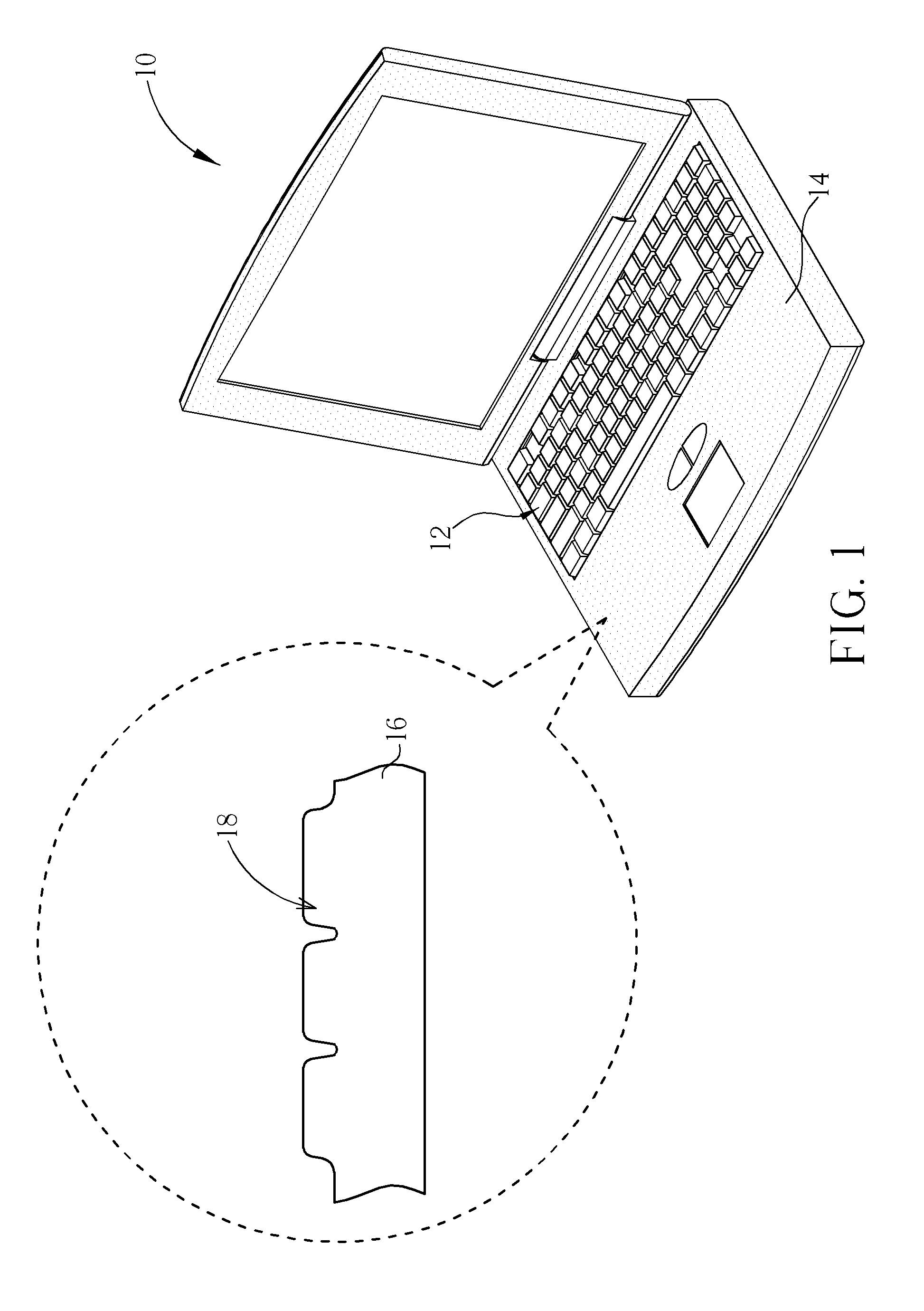
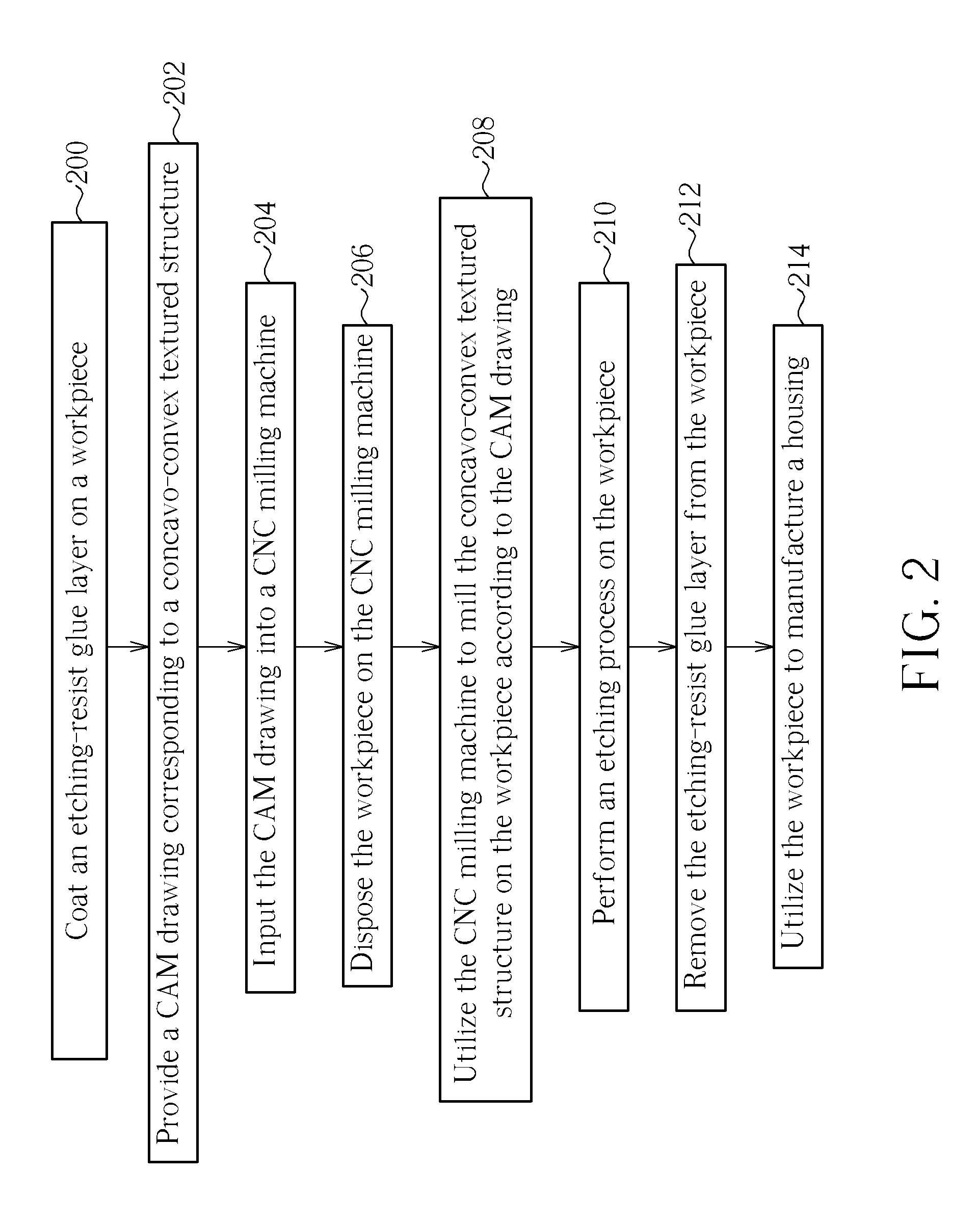
[0023]Please refer to FIG. 1, which is a diagram of an electronic device 10 according to a first preferred embodiment of the present invention. As shown in FIG. 1, the electronic device 10 is a notebook, but the present invention is not limited thereto, meaning that the present invention may also be applied for other electronic device, such as a mobile phone, a PDA (Personal Digital Assistant), etc. The electronic device 10 includes a device body 12 and a housing 14. In the present invention, the device body 12 is regarded as the combination of other components (e.g. a keyboard, an LCD monitor, a motherboard, etc.) besides the housing 14 in the electronic device 10. The housing 14 is disposed on the device body 12 for protection of the device body 12. The housing 14 includes a main body 16 and a concavo-convex textured structure 18. As shown in FIG. 1, the concavo-convex textured structure 18 is formed on the main body 16. In the present invention, a CNC milling process is utilized ...


PUM

PropertyMeasurementUnit
matt-surface textureaaaaaaaaaa
timeaaaaaaaaaa
structureaaaaaaaaaa

Abstract

A method is used for forming a concavo-convex textured structure on a housing of an electronic device. The method includes providing a CAM (Computer-Aided Manufacturing) drawing corresponding to the concavo-convex textured structure, inputting the CAM drawing into a CNC (Computer Numerical Control) milling machine, disposing a workpiece on the CNC milling machine, and utilizing the CNC milling machine to mill the concavo-convex textured structure on the workpiece according to the CAM drawing, and utilizing the workpiece to manufacture the housing of the electronic device.

Description

BACKGROUND OF THE INVENTION[0001]1. Field of the Invention[0002]The present invention relates to a method for forming a concavo-convex textured structure on a housing of an electronic device and related structures, and more specifically, to a method for forming a concavo-convex textured structure on a housing of an electronic device and related structures by a CNC milling process.[0003]2. Description of the Prior Art[0004]In recent years, a common method for forming a concavo-convex textured structure on a housing of an electronic device, such as a covering of a notebook computer, involves performing a chemical etching process on a surface of the housing. The said chemical etching process can be divided into two types: a direct etching method and an indirect etching method. The direct etching method involves coating an etching resist layer on a workpiece, utilizing a UV exposure process to form an etching mask on the workpiece, and performing a chemical etching process on the workpi...

Claims


Application Information

Patent Timeline
Patent Type & Authority Applications(United States)
IPC IPC(8): G05B19/4097G05B19/19C23F1/00B24C1/00H05K5/00
CPCG05B19/4097G05B2219/45145G05B2219/35084
Inventor HSIEH, CHEN-FENGHSIAO, YA-CHI
Owner WISTRON CORP
Why Eureka
Try Eureka