Chip device, multi-layered chip device and method of producing the same

Inactive Publication Date: 2014-01-23
SAMSUNG ELECTRO MECHANICS CO LTD
View PDF6 Cites 14 Cited by
  • Summary
  • Abstract
  • Description
  • Claims
  • Application Information

AI Technical Summary

Benefits of technology

[0010]Another aspect of the present invention provides a chip device with excellent induct

Problems solved by technology

Meanwhile, as electronic devices become slim and light, demand fo

Method used


Image

  • Chip device, multi-layered chip device and method of producing the same
  • Chip device, multi-layered chip device and method of producing the same
  • Chip device, multi-layered chip device and method of producing the same

Examples


Example

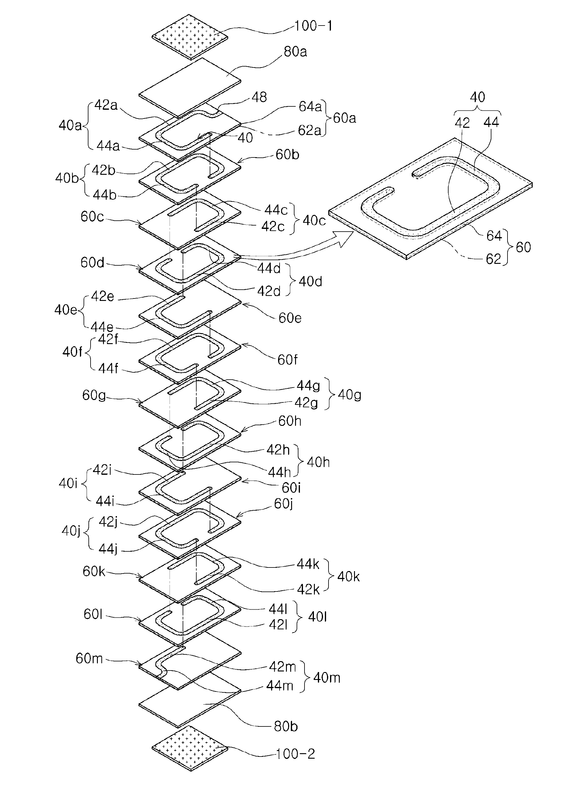
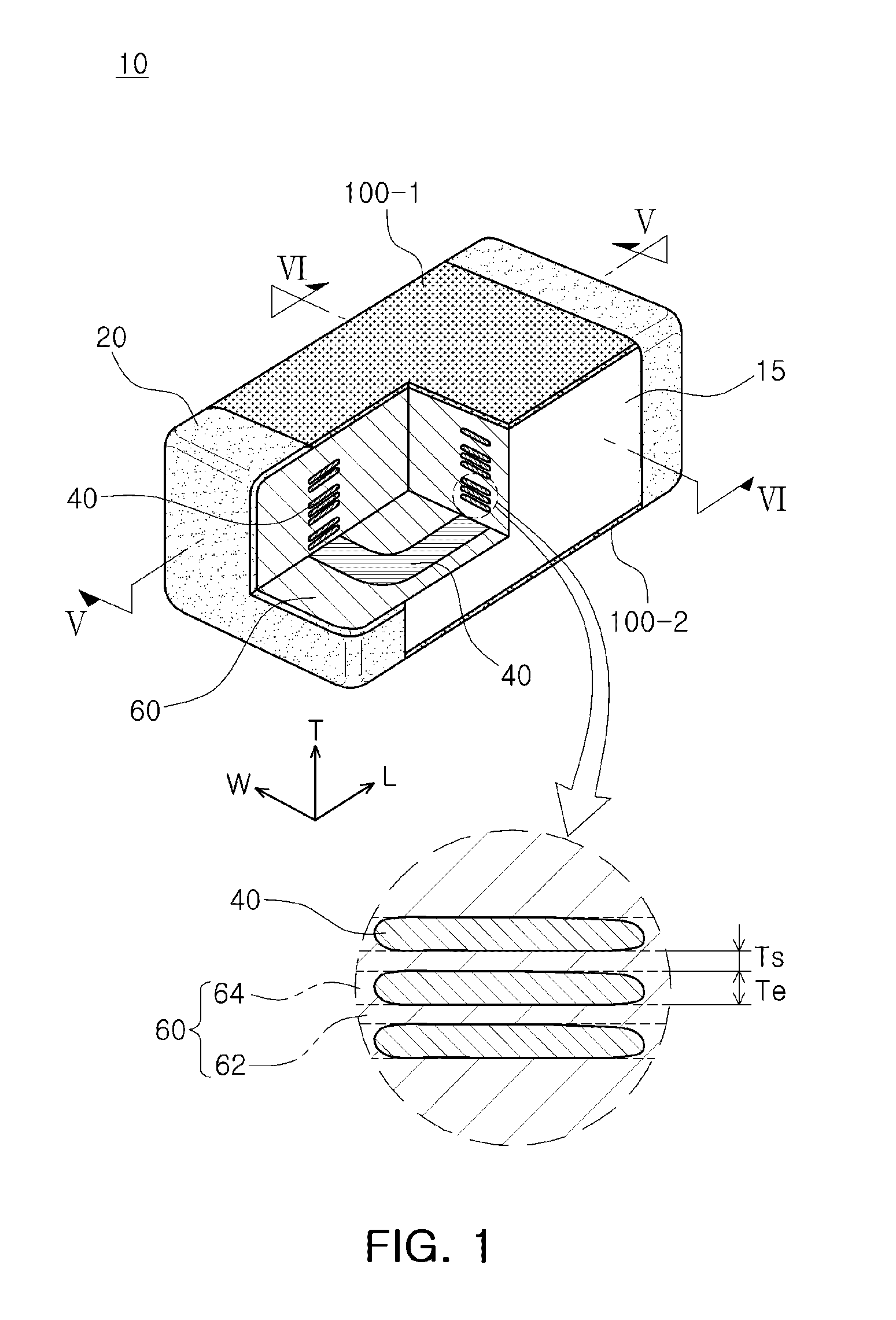
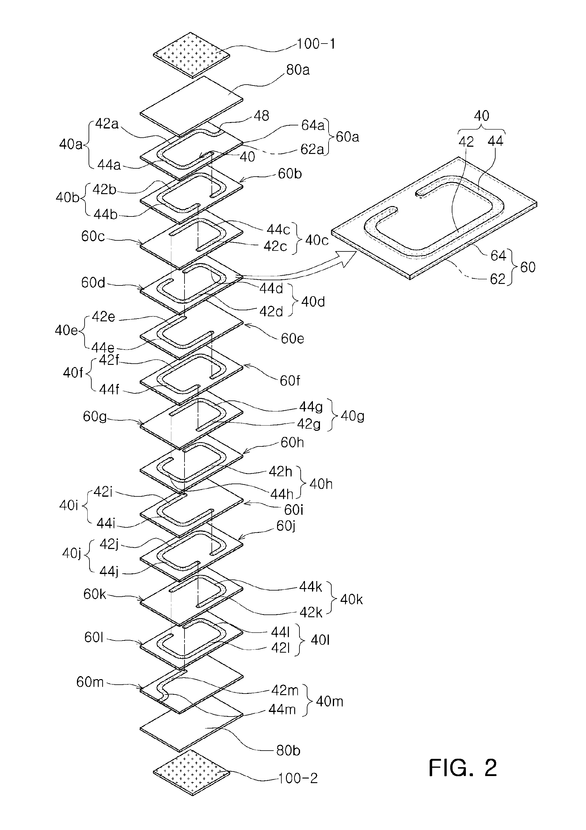
[0025]Hereinafter, embodiments of the present invention will be described in detail with reference to the accompanying drawings. The invention may, however, be embodied in many different forms and should not be construed as being limited to the embodiments set forth herein. Rather, these embodiments are provided so that this disclosure will be thorough and complete, and will fully convey the scope of the invention to those skilled in the art. In the drawings, the shapes and dimensions of elements may be exaggerated for clarity, and the same reference numerals will be used throughout to designate the same or like elements.

[0026]In addition, singular forms used in the specification are intended to include plural forms unless the context clearly indicates otherwise. In the specification, it is to be noted that the terms “comprising” or “including”, and the like, are not to be construed as necessarily including several components or several steps described in the specification, and some...


PUM

PropertyMeasurementUnit
Widthaaaaaaaaaa
Widthaaaaaaaaaa
Lengthaaaaaaaaaa

Abstract

There is provided a multi-layered chip device, including: a multi-layered body in which a plurality of inner magnetic layers are stacked; an inner electrode layer formed within the multi-layered body; an outer magnetic layer stacked on at least one of an upper surface and a lower surface of the multi-layered body; and external electrodes formed on outside of the multi-layered body and the outer magnetic layer and electrically connected to the inner electrode layer, wherein a length of the outer magnetic layer is shorter than the inner magnetic layer.

Description

CROSS-REFERENCE TO RELATED APPLICATIONS[0001]This application claims the priority of Korean Patent Application No. 10-2012-0078422 filed on Jul. 18, 2012, in the Korean Intellectual Property Office, the disclosure of which is incorporated herein by reference.BACKGROUND OF THE INVENTION[0002]1. Field of the Invention[0003]The present invention relates to a chip device, a multi-layered chip device, and a method of producing the same.[0004]2. Description of the Related Art[0005]An inductor, a multi-layered chip component, is a representative passive element capable of removing noise from a signal by being included in an electronic circuit together with a resistor and a capacitor.[0006]A multi-layered chip type inductor may be manufactured by printing and stacking conductive patterns so as to form a coil within a magnetic substance or a dielectric substance. The multi-layered chip inductor has a structure in which a plurality of magnetic layers on which conductive patterns are formed ar...

Claims


Application Information

Patent Timeline
IPC IPC(8): H01F17/00H01F41/00
CPCH01F17/0013H01F41/00H01F17/0033H01F27/292H01F41/046Y10T29/4902H01F17/00
Inventor PARK, SANG SOOAHN, YOUNG GHYUPARK, MIN CHEOL
Owner SAMSUNG ELECTRO MECHANICS CO LTD
Why Eureka
Try Eureka