Pixel matrix, touch display device and drving method thereof

a touch display device and pixel matrix technology, applied in semiconductor devices, instruments, computing, etc., can solve problems such as serious interference between them, achieve the effects of reducing the coupling effect, reducing the overall thickness of the touch display device, and improving the aperture ratio

a touch display device and pixel matrix technology, applied in semiconductor devices, instruments, computing, etc., can solve problems such as serious interference between them, achieve the effects of reducing the coupling effect, reducing the overall thickness of the touch display device, and improving the aperture ratio

US20140333571A1Active Publication Date: 2014-11-13HIMAX TECH LTD

Image

  • Pixel matrix, touch display device and drving method thereof
  • Pixel matrix, touch display device and drving method thereof
  • Pixel matrix, touch display device and drving method thereof

Examples


Embodiment Construction

[0020]Reference will now be made in detail to the present preferred embodiments of the invention, examples of which are illustrated in the accompanying drawings. Wherever possible, the same reference numbers are used in the drawings and the description to refer to the same or like parts.

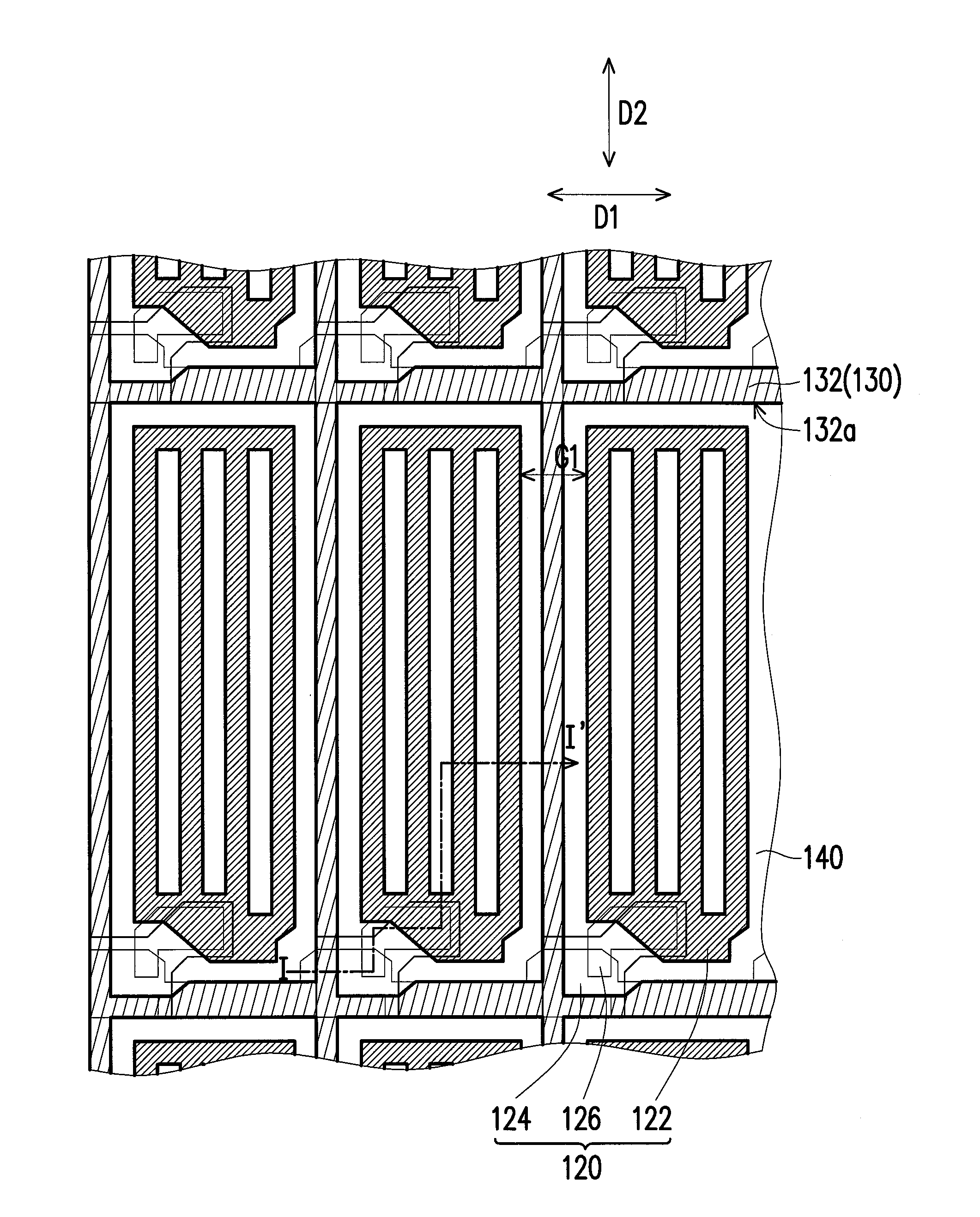
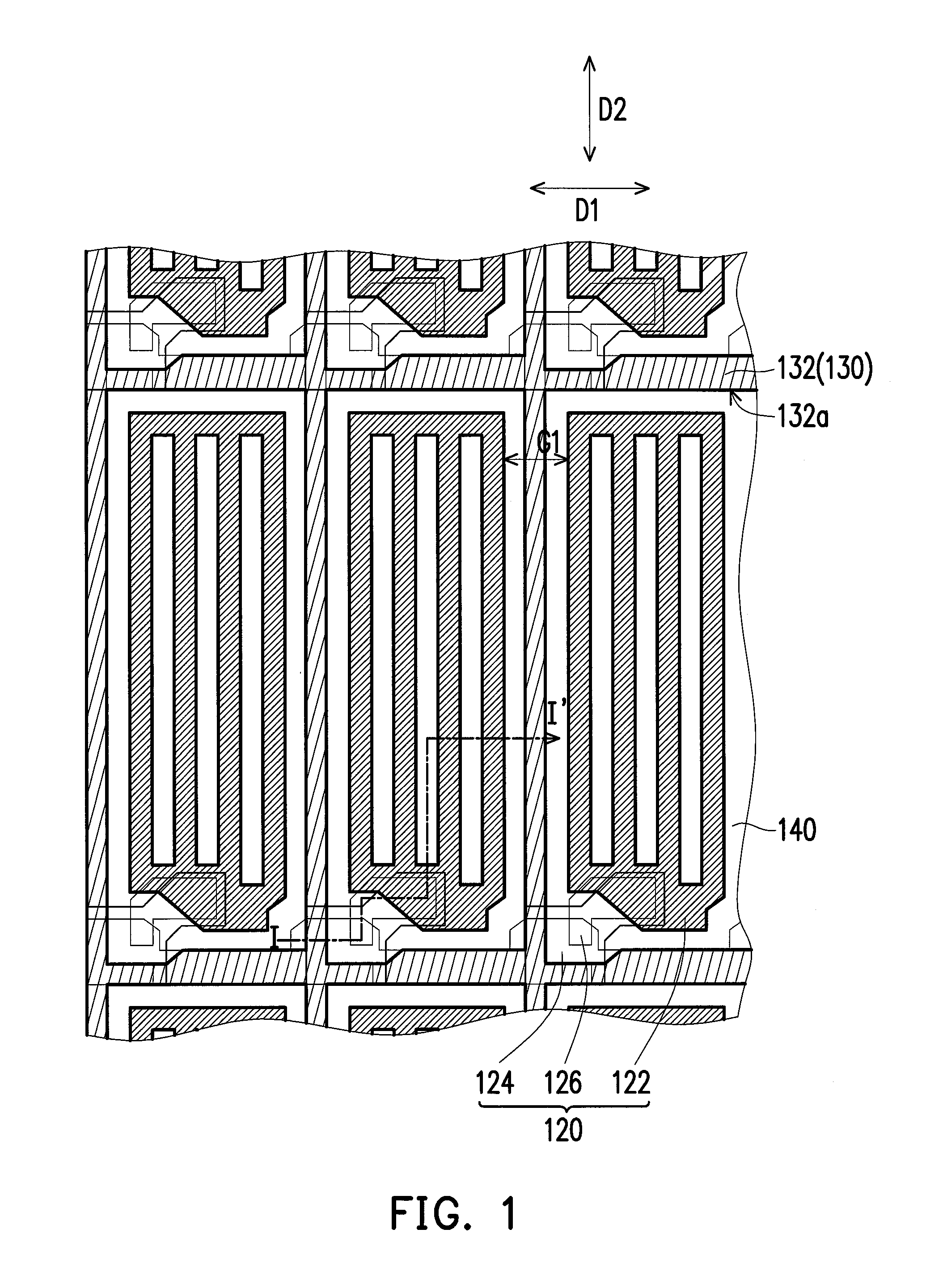
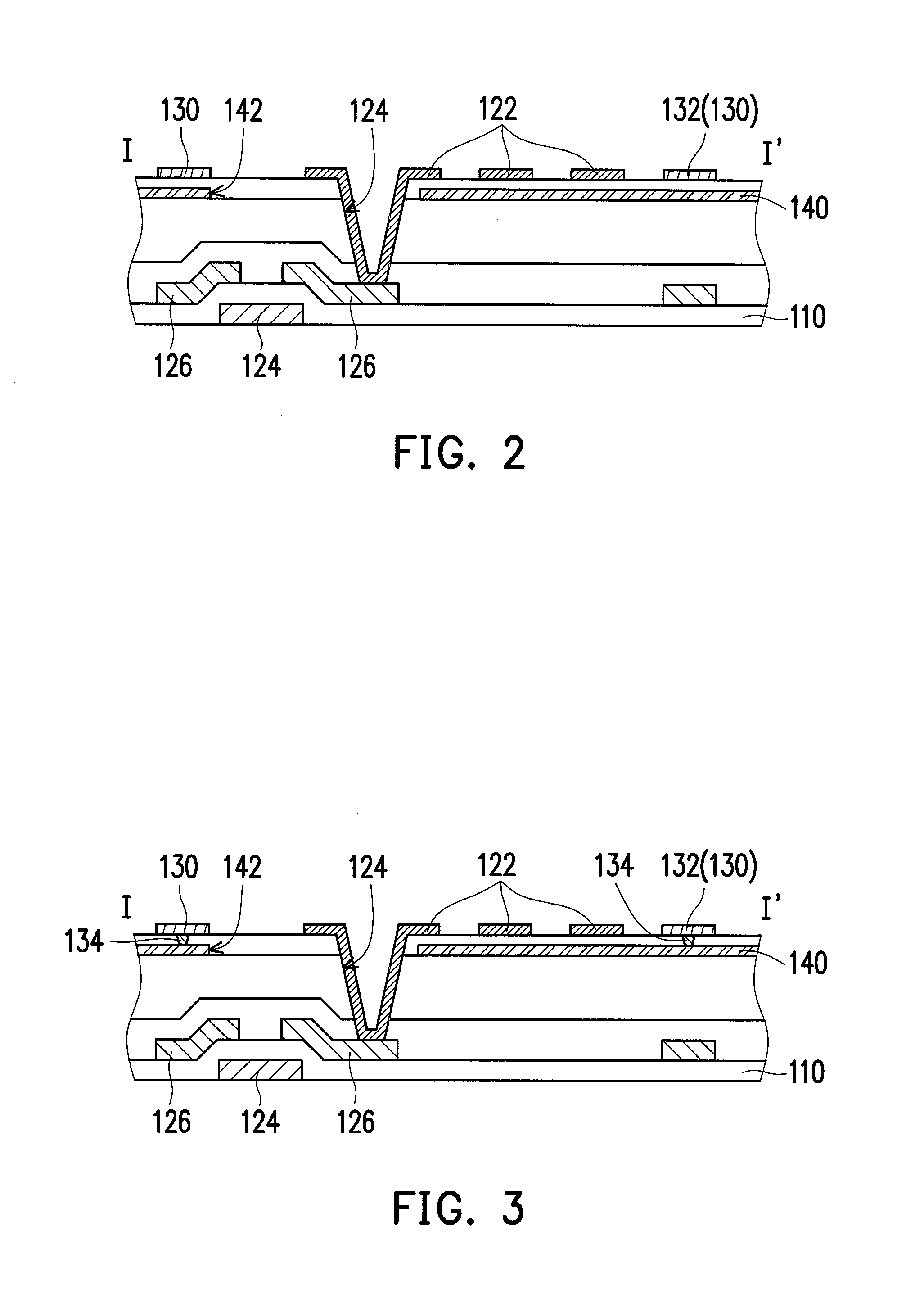
[0021]FIG. 1 illustrates a schematic top view of a pixel matrix according to an embodiment of the invention. FIG. 2 illustrates a cross-sectional view of the pixel matrix in FIG. 1 along section line I-I′. In the present embodiment, the pixel matrix as shown in FIG. 1 and FIG. 2 includes a first substrate 110, a plurality of pixel structures 120, a first electrode set 130 and a common electrode 140. The pixel structures 120 include a plurality of pixel electrodes 122 and are disposed on the first substrate 110 in an array arrangement. In detail, the pixel structures 120 further include a plurality of active devices (not shown), a plurality of scan lines 124 and a plurality of data lines 126. The acti...


PUM


Abstract

A pixel matrix including a first substrate, a plurality of pixel structures, a first electrode set and a common electrode is provided. The pixel structures are disposed on the first substrate in an array arrangement. Each of the pixel structures includes a pixel electrode. The first electrode set includes a plurality of first electrodes arranged along a first direction on the first substrate. Each of the first electrodes having a plurality of first openings arranged corresponding to the pixel electrodes and surrounding the corresponding pixel electrodes. The common electrode is disposed between the first electrodes and the first substrate and between the pixel electrode and the first substrate. A touch display device having the pixel matrix and the driving method thereof are also provided.

Description

CROSS-REFERENCE TO RELATED APPLICATION[0001]This application claims the priority benefits of U.S. provisional application Ser. No. 61 / 822,894, filed on May 13, 2013. The entirety of the above-mentioned patent applications is hereby incorporated by reference herein and made a part of this specification.BACKGROUND OF THE INVENTION[0002]1. Field of the Invention[0003]The invention generally relates to a pixel matrix, display device and a driving method. More particularly, the invention relates to a pixel matrix, touch display device and a driving method thereof.[0004]2. Description of Related Art[0005]A display apparatus having a touch-sensing function is generally implemented by a touch system and a display system independent to each other. System integration and cost reduction are unchanged developing trends of electronics industry. With progress of fabrication techniques, a touch panels is now successfully integrated with a display panel, so that a user can direct an electronic devi...

Claims


Application Information

Patent Timeline
13 Nov 2014
Publication
US20140333571A1
IPC
G06F3/041; H01L23/48
CPC
G06F3/0412; H01L23/48; G06F3/04184; G06F3/0445; G06F3/0446; H01L27/124; G06F3/0416; G06F3/044
Inventors
HU, CHIA-WEI