
RF power transistor
a power transistor and radio frequency technology, applied in the direction of basic electric elements, electrical appliances, semiconductor devices, etc., can solve the problems of reducing the transconductance, deteriorating the device performance, and unsatisfactory dc-to-rf dispersion
- Summary
- Abstract
- Description
- Claims
- Application Information
AI Technical Summary
Benefits of technology
Problems solved by technology
Method used
Image

Examples
first embodiment
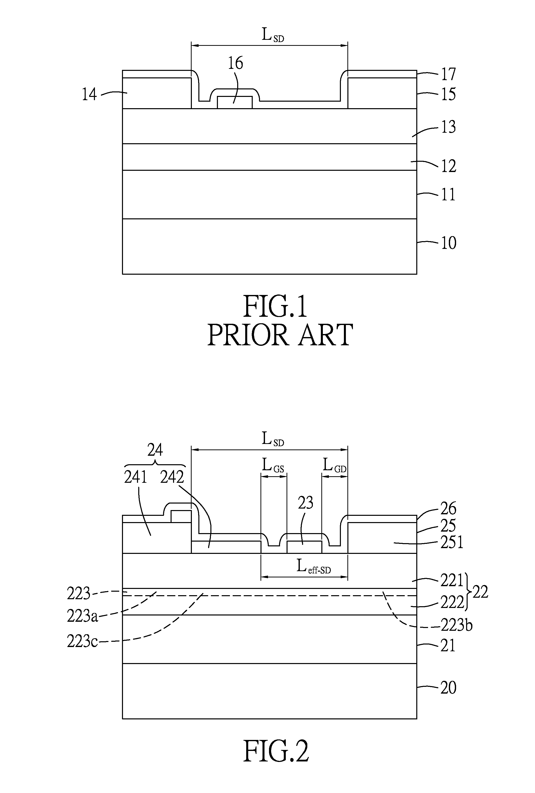
[0014]FIG. 2 illustrates an RF power transistor according to the present invention.
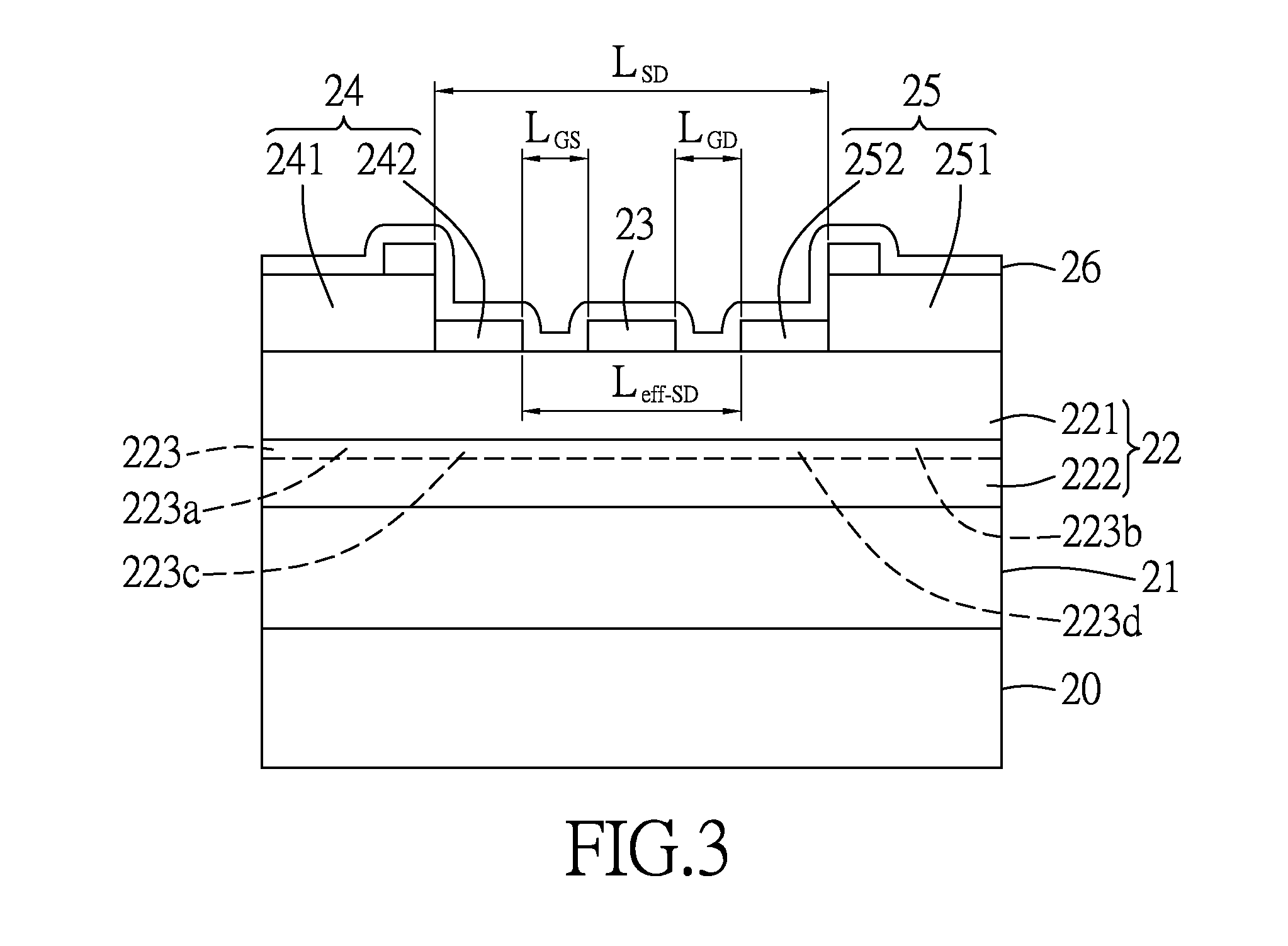
[0015]The RF power transistor is a GaN-based high electron mobility transistor (HEMT), and includes: a substrate 20; a buffer layer 21 formed on the substrate 20; a III-N-type semiconductor heterostructure 22 that is formed on the buffer layer 21, that includes an undoped barrier layer 221 and an active layer 222, and that is formed with a continuous two dimensional electron gas (2DEG) channel 223 disposed at one side of the active layer 222 which is adjacent to the barrier layer 221, the 2DEG channel 223 having an ohmic source-aligned region 223a, an ohmic drain-aligned region 223b, and a first Schottky-aligned region 223c that is disposed between the ohmic source-aligned and drain-aligned regions 223a, 223b; a gate electrode 23 that is formed on the semiconductor heterostructure 22 and that is disposed over the barrier layer 221; source and drain electrodes 24, 25 formed on the barrier layer 221; an...
second embodiment
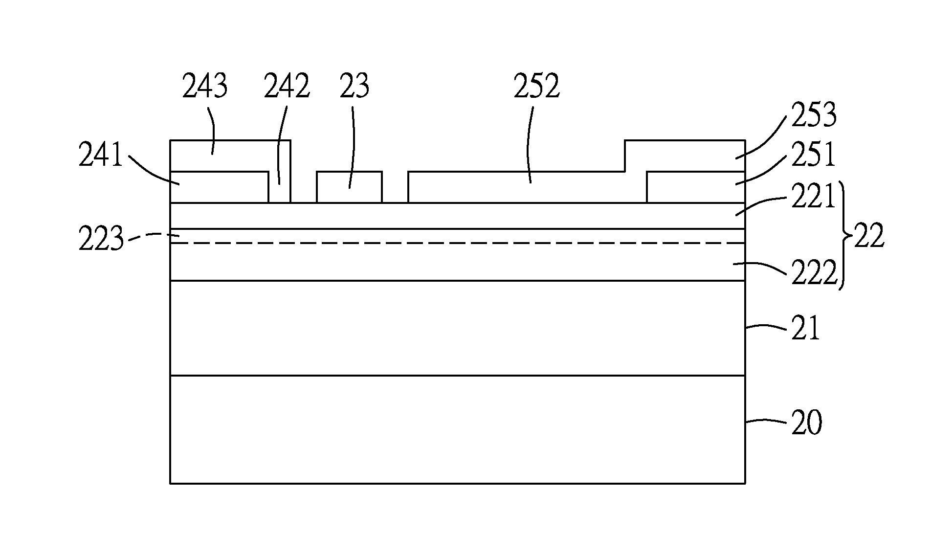
[0029]FIGS. 4A to 4I illustrate consecutive steps of a method of making an embodiment of the RF power transistor that has a structure similar to that of the The method includes: forming a buffer layer 21 on a substrate 20 using metal-organic chemical vapor deposition (MOCVD) or molecular beam epitaxy (MBE) technologies (see FIG. 4A); forming an active layer 222 on the buffer layer 21 using MOCVD or MBE technologies (see FIG. 4B); forming a barrier layer 221 on the active layer 222 using MOCVD or MBE technologies (see FIG. 4C), a 2DEG channel 223 being induced in the active layer 222 due to the heterostructure between the barrier layer 221 and the active layer 222; forming source and drain ohmic contacts 241, 251 on the barrier layer 221 using physical vapor deposition (see FIG. 4D), followed by annealing under 850° C.; forming a Schottky-contact layer 28 of a metal stack on the ohmic contacts 241, 251 of the source and drain electrodes 24, 25 and the barrier layer 221 using physica...
PUM
 Abstract
Description
Claims
Application Information