Pixel electrode, array substrate and display panel

a technology of array substrate and pixel electrode, which is applied in the field of display technologies, can solve the problems of aggravating acoustic crosstalk and screen flickering on the display device, affecting so as to improve the quality of displayed images, reduce acoustic crosstalk and screen flickering, and increase storage capacitance

Active Publication Date: 2016-06-30
XIAMEN TIANMA MICRO ELECTRONICS +1
View PDF3 Cites 0 Cited by
  • Summary
  • Abstract
  • Description
  • Claims
  • Application Information

AI Technical Summary

Benefits of technology

[0009]A pixel electrode, an array substrate including the pixel electrode and a display panel including the array substrate are provided according to embodiments of the present disclosure, for increasing a storage capacitance between the pixel electrode and a common electrode in the display panel, alleviating acoustic crosstalk and screen flickering occurring in the display panel, and improving the quality of displayed images.

Problems solved by technology

At instants when the thin film transistor is turned on and turned off, variation of a voltage of the gate line may affect a voltage of the pixel electrode via the parasitic capacitor Cgs, and a feed though voltage is generated on the pixel electrode, thereby affecting the quality of displayed images.
As can be seen from the above formula, the overlapping area of the pixel electrode and the common electrode may decrease as the area of the pixel electrode decreases, and the feed though voltage on the pixel electrode may increase correspondingly, thereby aggravating acoustic crosstalk and screen flickering occurring on the display device and affecting quality of displayed images.

Method used


Image

  • Pixel electrode, array substrate and display panel
  • Pixel electrode, array substrate and display panel
  • Pixel electrode, array substrate and display panel

Examples


Embodiment Construction

[0037]To make the above features and advantages of the disclosure more obvious and easier to be understood, in the following, specific embodiments of the disclosure are illustrated in detail in conjunction with drawings.

[0038]Specific details are set forth in the following descriptions for a better understanding of the disclosure. The disclosure may also be implemented in other ways different from those described herein, and similar extensions can be made by those skilled in the art without departing from the spirit of the disclosure. Therefore, the disclosure is not limited to the embodiments disclosed hereinafter.

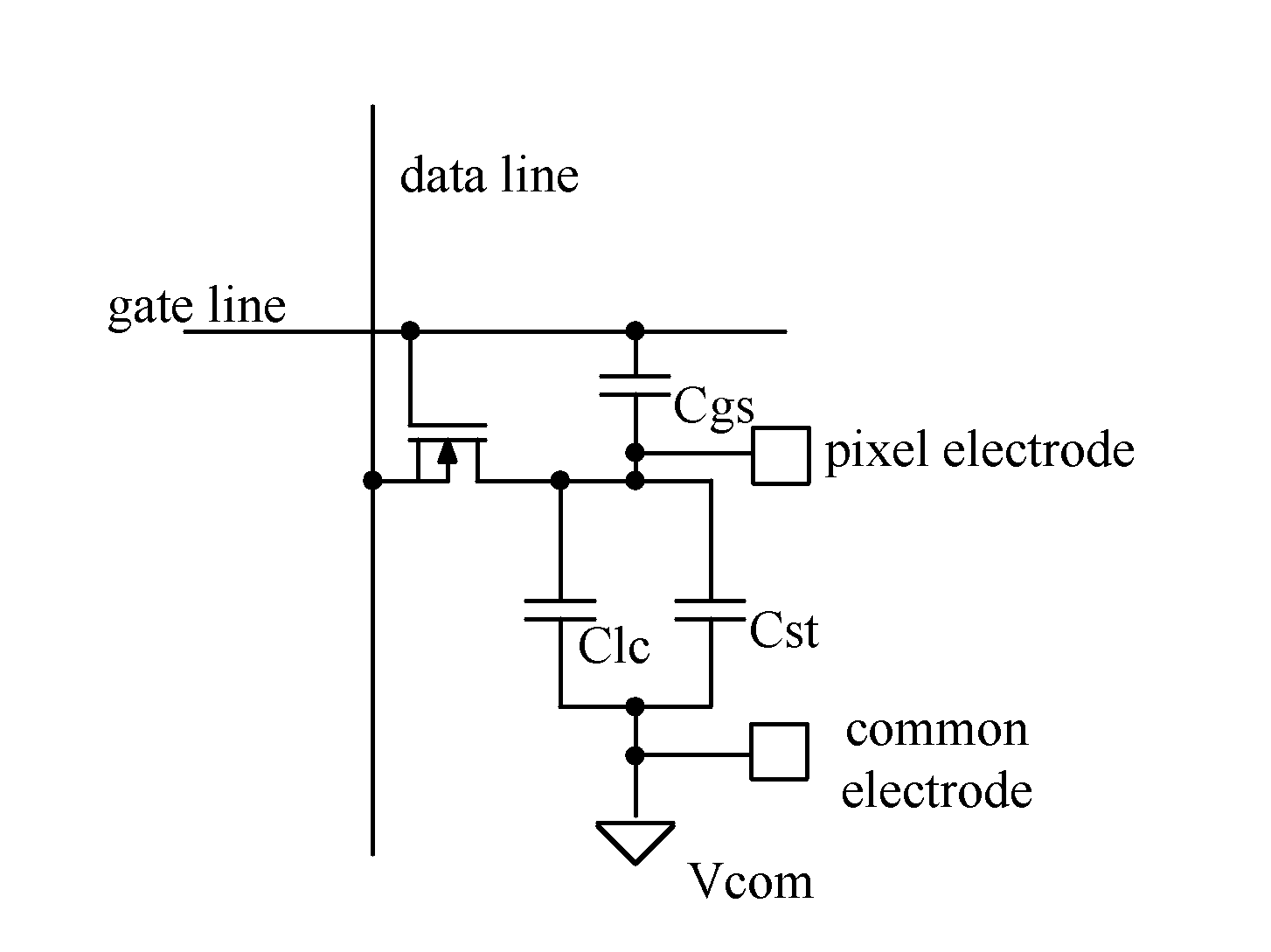
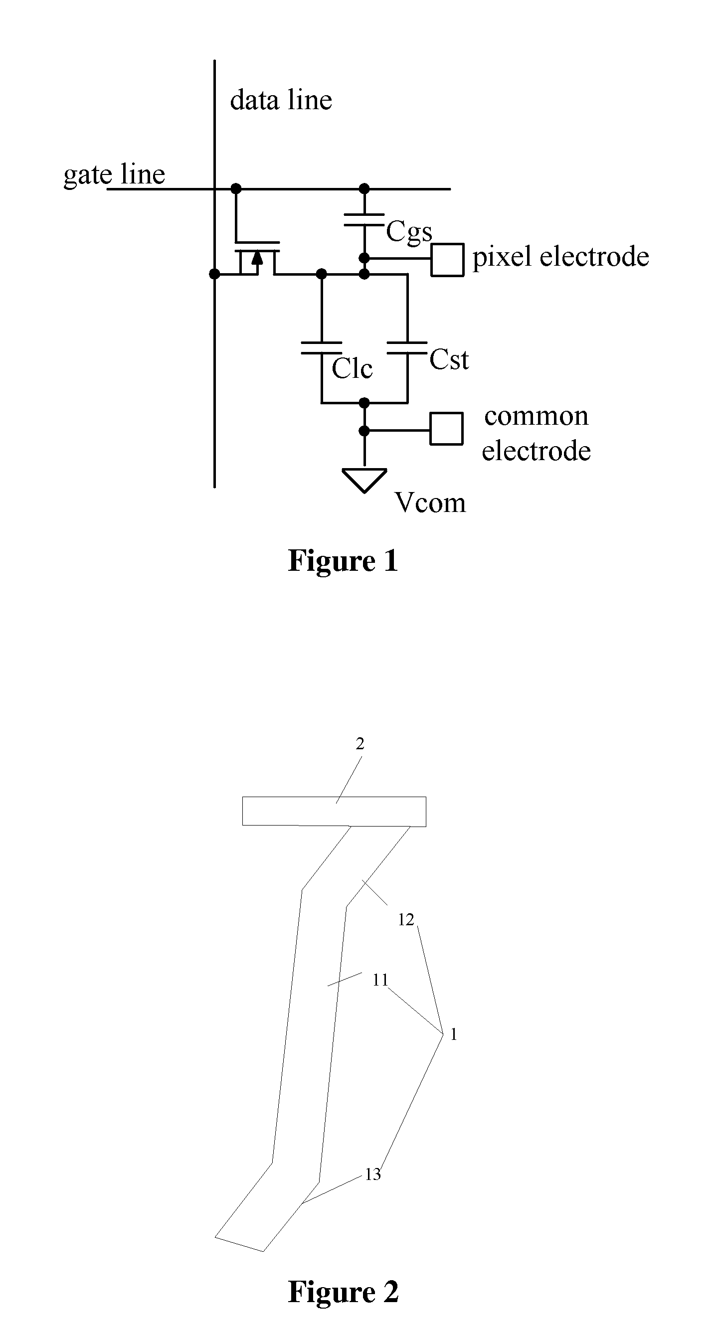
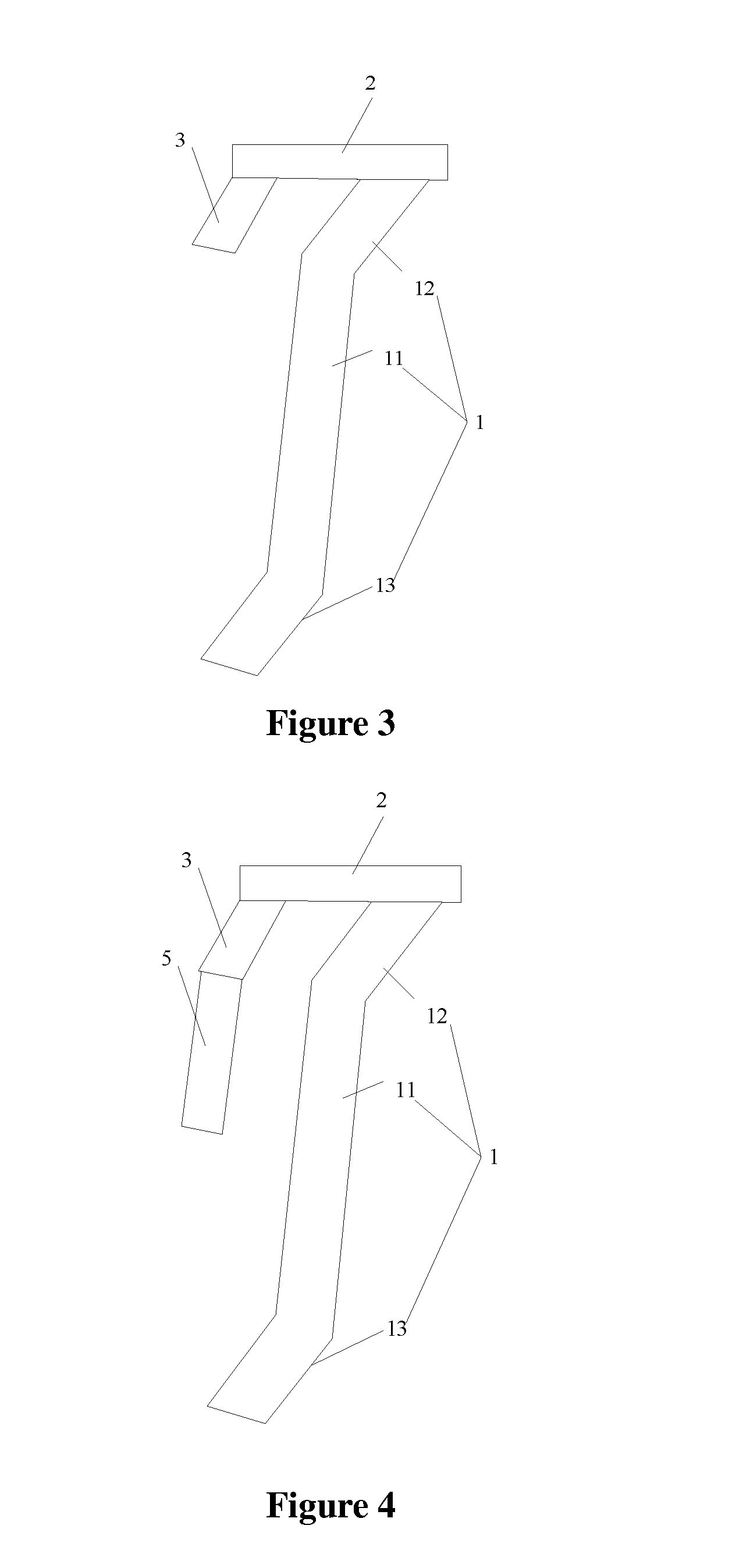
[0039]A pixel electrode is provided according to an embodiment of the present disclosure. As shown in FIG. 2, the pixel electrode includes a main pixel electrode 1 extending in a first direction and a first extending portion 2. The main pixel electrode 1 includes a main electrode 11, and a first end portion 12 and a second end portion 13 respectively located at two ends o...


PUM

PropertyMeasurementUnit
angleaaaaaaaaaa
distanceaaaaaaaaaa
widthaaaaaaaaaa

Abstract

A pixel electrode, an array substrate and a display panel are provided. The pixel electrode includes: a main pixel electrode extending in a first direction and a first extending portion. The main pixel electrode includes a main electrode, and a first end portion and a second end portion respectively located at two ends of the main electrode. The first extending portion extends in a second direction and is connected to the first end portion. The second direction intersects with the first direction. In addition to the main pixel electrode, the pixel electrode further includes the first extending portion electrically connected to the first end portion of the main pixel electrode. The area of the pixel electrode is increased due to the arrangement of the extending portion

Description

CROSS REFERENCE TO RELATED APPLICATIONS[0001]The present application claims the priority to Chinese Patent Application No. 201410814863.2, entitled “PIXEL ELECTRODE, ARRAY SUBSTRATE AND DISPLAY PANEL”, filed on Dec. 24, 2014 with the State Intellectual Property Office of People's Republic of China, which is incorporated herein by reference in its entirety.FIELD OF THE DISCLOSURE[0002]The disclosure relates to displaying technologies, and in particular, to a pixel electrode, an array substrate including the pixel electrode and a display panel including the array substrate.BACKGROUND OF THE DISCLOSURE[0003]With the development of displaying techniques, the number of pixels per inch in a display device increases, a distance between adjacent pixels decreases, and correspondingly, a ratio of the area of a pixel electrode over the area of the pixel decreases.[0004]Reference may be made to FIG. 1, which schematically illustrates a principle of connections within the pixel of a conventional...

Claims


Application Information

Patent Timeline
Patent Type & Authority Applications(United States)
IPC IPC(8): G02F1/1362G02F1/1343G02F1/1335G02F1/1368
CPCG02F1/136213G02F1/1368G02F2001/134345G02F1/133514G02F1/134309G02F1/136286H01L27/1214G02F1/134345G02F1/134363
Inventor MA, YANGZHAOSHEN, POPINGWU, LING
Owner XIAMEN TIANMA MICRO ELECTRONICS
Why Eureka
Try Eureka