TFT array having conducting lines with low resistance

a technology of conducting lines and arrays, which is applied in the field of display panels, can solve the problems of reducing the charging efficiency of display pixels, addressing line resistance becoming very high, and capacitance loading, so as to enhance the transconductance of switching elements and enhance storage capacitan

Active Publication Date: 2018-11-15
A U VISTA INC
View PDF0 Cites 0 Cited by
  • Summary
  • Abstract
  • Description
  • Claims
  • Application Information

AI Technical Summary

Benefits of technology

[0004]The present invention provides a pixel structure in a display panel. The pixel structure includes a switching element and a storage capacitor formed on a substrate. The switching element has a gate electrode, a semiconductor layer and a high-k dielectric layer between the gate electrode and the semiconductor layer to enhance the transconductance of the switching element. The storage capacitor has a first storage capacitor electrode, a second storage capacitor electrode and a high-k dielectric layer between the first and second storage capacitor electrodes to enhance the storage capacitance. The high-k dielectric layer has a dielectric constant equal to or greater than 8. The switching element also has a drain electrode and a source electrode disposed on the semiconductor layer. The pixel structure also has a plurality of conducting lines to provide a common line, a gate line and a source line. The gate line electrically connected to the gate electrode; the source line electrically connected to the source electrode and the common line electrically connected to the storage capacitor. The substrate has a plurality of groove made thereon filled with a conducting material to provide the conducting lines. The common line and the gate line are arranged in the first direction on the substrate and the source line is arranged in the different second direction. The source line is segmented into source line segments and a source connector is used to provide electrical connection between two adjacent source line segments and the cross-over above the common line and the gate line. A low-k dielectric layer is used at the cross-over, wherein the low-k dielectric layer has a dielectric constant equal to or lower than 3.5.

Problems solved by technology

As the size of the TFT-driven display panel becomes large and its resolution becomes high, the addressing time of the pixels becomes very short, the line resistance of the addressing lines becomes very high, and the capacitance loading of the display panel becomes high, causing the charging efficiency of the display pixel to decrease significantly.
It is a recognized issue to lower the addressing line resistance and the capacitance loading, and to increase the TFT transconductance for the TFT array.

Method used


Image

  • TFT array having conducting lines with low resistance
  • TFT array having conducting lines with low resistance
  • TFT array having conducting lines with low resistance

Examples


Embodiment Construction

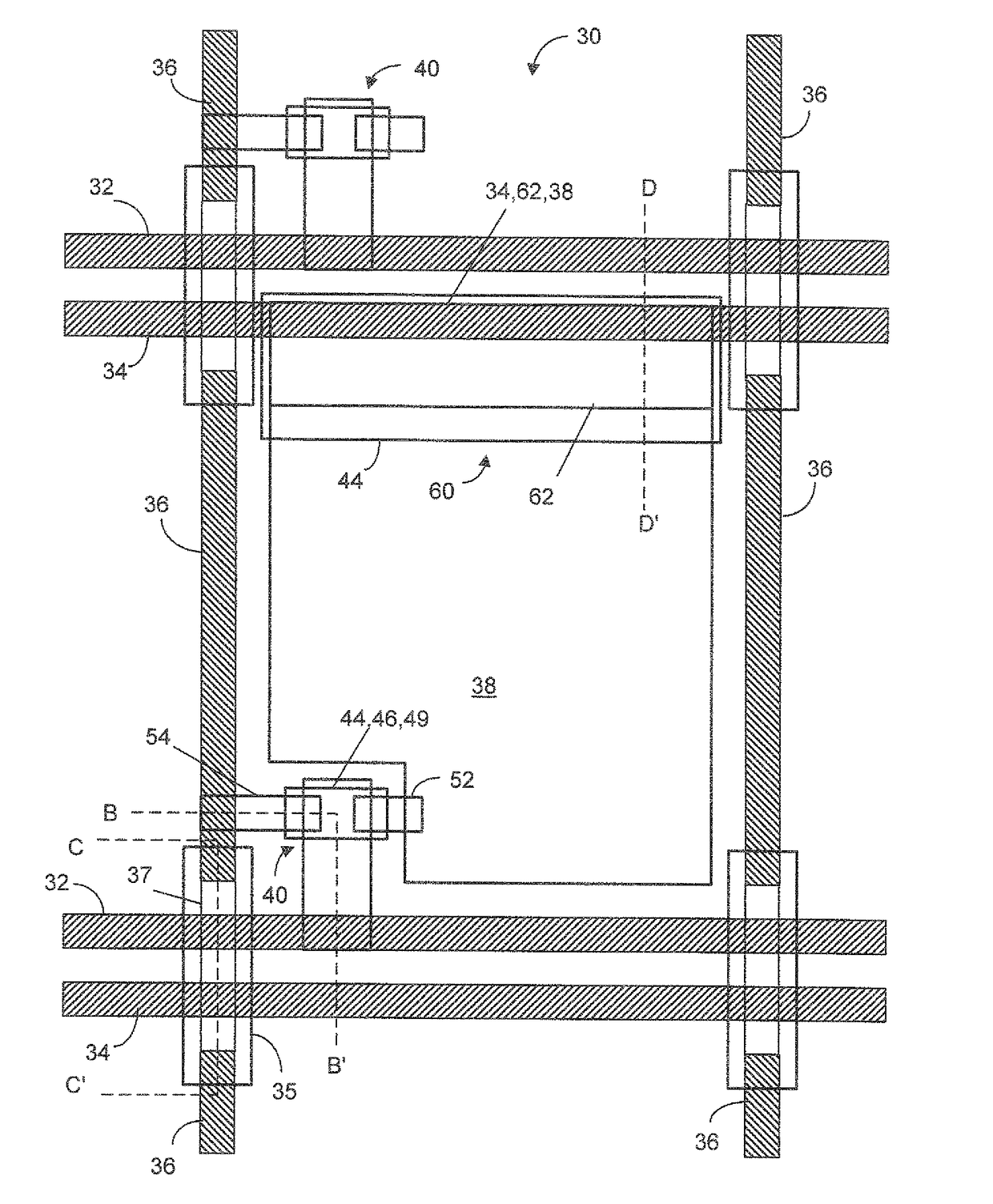
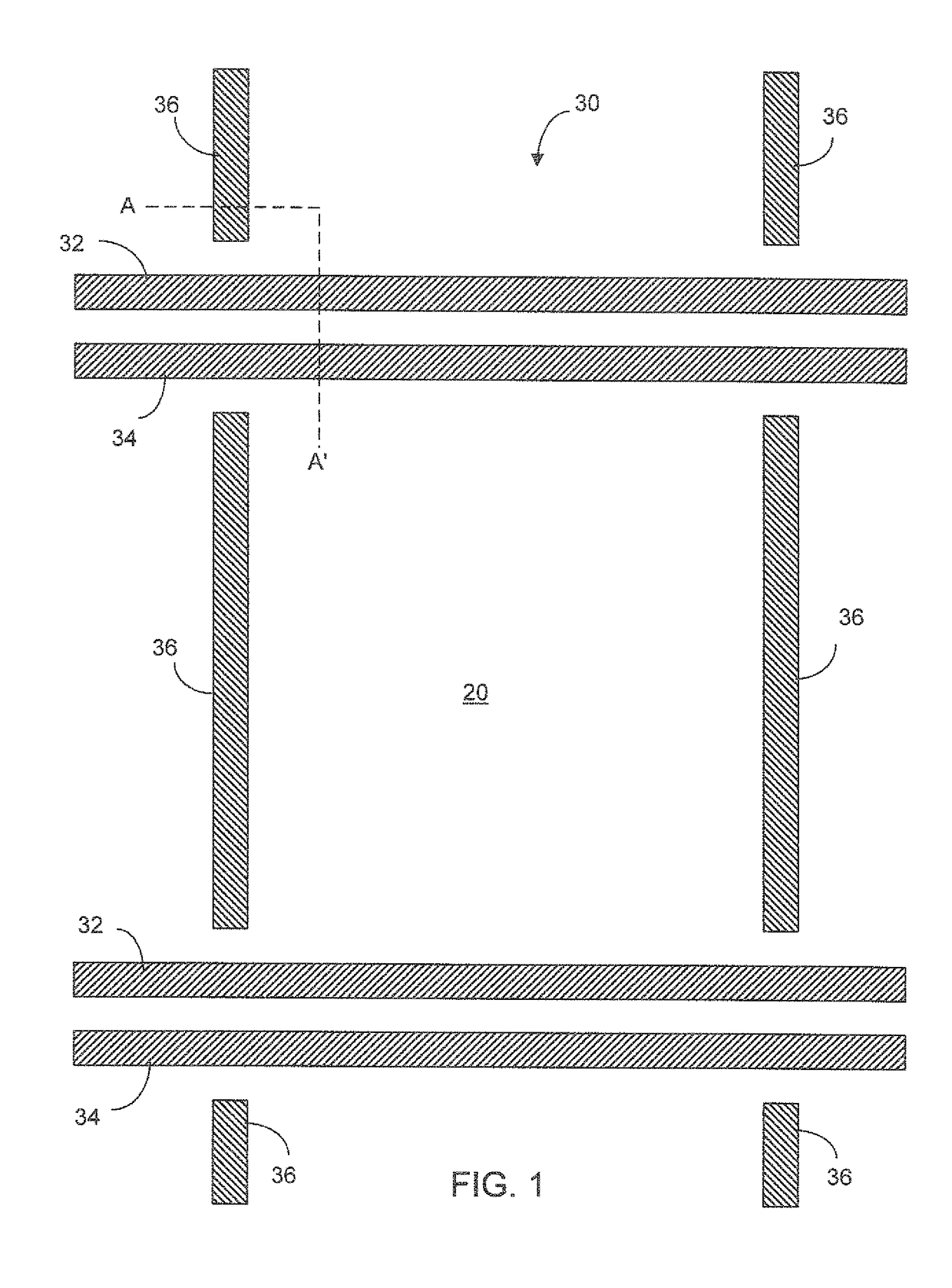
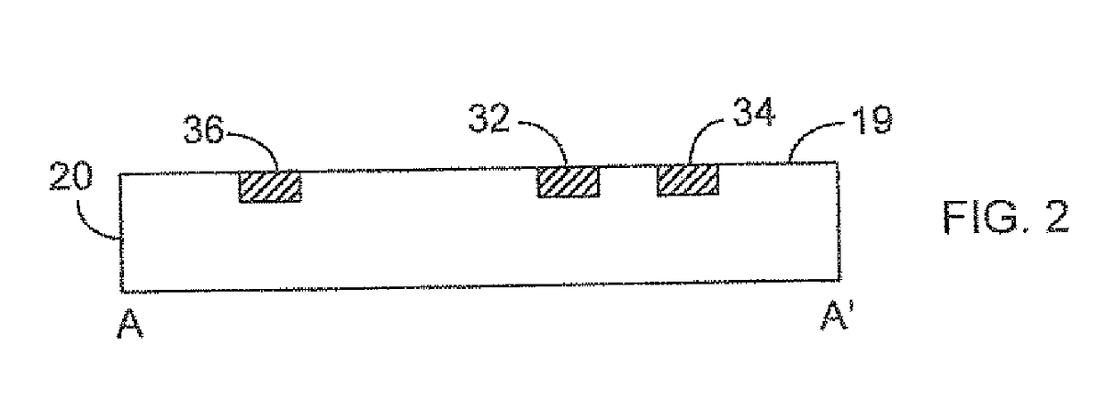
[0081]The present invention provides a pixel structure in a pixel for used in a display panel that reduces the line resistance. According to various embodiments of the present invention, the substrate of the display panel comprises a plurality of grooves made on the substrate and a plurality of conducting lines formed in the grooves. The conducting line can be made from a silver or copper conductive ink to provide a low-resistance line served as a gate line, common line or source line. Alternatively, the conducting line can be made from electroless printing copper. In a pixel having a storage capacitor and a TFT with a gate electrode, a source electrode and a drain electrode, the gate electrode is connected to a gate line, a source electrode is connected to a source line, and one of the capacitor electrodes in the storage capacitor is connected to a common line. According to an embodiment of the present invention, at least part of one or more of the gate electrode, the source electr...


PUM

PropertyMeasurementUnit
dielectric constantaaaaaaaaaa
thicknessaaaaaaaaaa
thicknessaaaaaaaaaa

Abstract

A pixel structure in a pixel for used in a display panel has a plurality of grooves made on a substrate and a plurality of conducting lines formed in the grooves. The conducting line can be made from a silver or copper conductive ink to provide a low-resistance line served as a gate line, common line or source line. In a pixel having a storage capacitor and a TFT with a gate electrode, a source electrode and a drain electrode, the gate electrode is connected to a gate line and a source electrode and one of the capacitor electrodes in the storage capacitor is connected to a common line. At least part of one or more of the gate electrode and the source electrode is disposed on top of and in contact with the surface of one or more conducting lines.

Description

TECHNICAL FIELD[0001]The present invention relates generally to a display panel and, more specifically, to an active matrix substrate having a TFT array for driving the display panel.BACKGROUND OF THE INVENTION[0002]A display panel generally has a large number of pixels arranged in a two dimensional array. To drive the display panel, an active matrix substrate includes a large number of switching elements made of thin-film transistors or TFTs to activate the pixels.[0003]It is known in the art that each switching element has a drain electrode, a source electrode and a gate electrode and each pixel has a pixel electrode and a storage capacitor to store electric charges between the pixel electrode and a common line. As the size of the TFT-driven display panel becomes large and its resolution becomes high, the addressing time of the pixels becomes very short, the line resistance of the addressing lines becomes very high, and the capacitance loading of the display panel becomes high, ca...

Claims


Application Information

Patent Timeline
Patent Type & Authority Applications(United States)
IPC IPC(8): G02F1/1362G02F1/1368G02F1/1333
CPCG02F1/136286G02F1/1368G02F1/133345G02F2001/136295G02F2202/10G02F2001/136236H01L27/124H01L27/1225H01L27/1255G02F2001/13606H01L29/7869H01L27/1218G02F1/13629
Inventor LUO, FANG-CHENDEN BOER, WILLEMLEE, SEOK-LYUL
Owner A U VISTA INC
Why Eureka
Try Eureka