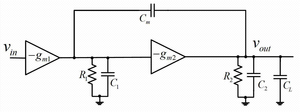
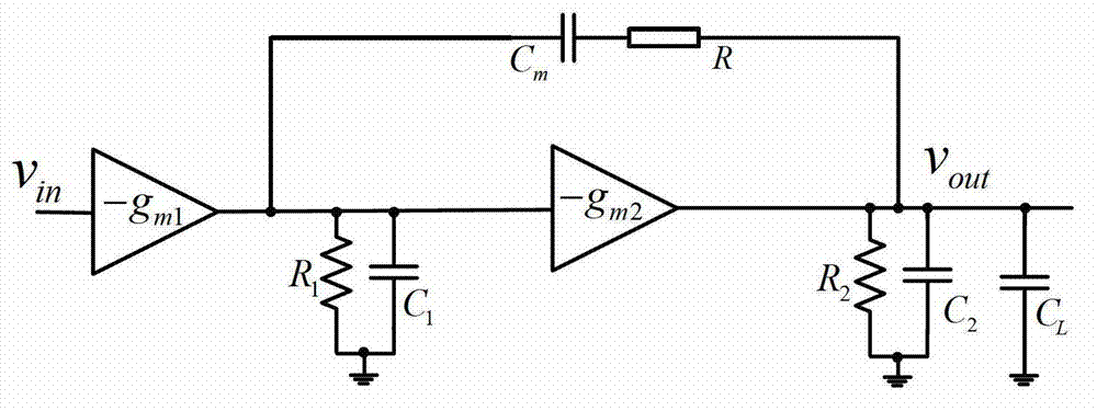
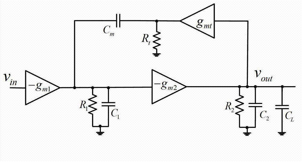
Split compensation two-stage operational amplifier based on inverter input structure

A technology of operational amplifier and input structure, which is applied in the field of electronics, can solve unconfirmed problems, achieve the effect of increasing slew rate, increasing gain and unity gain bandwidth, and increasing transconductance

Inactive Publication Date: 2013-07-10
UNIV OF ELECTRONICS SCI & TECH OF CHINA
View PDF2 Cites 15 Cited by
  • Summary
  • Abstract
  • Description
  • Claims
  • Application Information

AI Technical Summary

Problems solved by technology

But at present, the performance of operational amplifiers can be improved, and the reports of frequency compensation with strong robustness have not been verified.

Method used


Image

  • Split compensation two-stage operational amplifier based on inverter input structure
  • Split compensation two-stage operational amplifier based on inverter input structure
  • Split compensation two-stage operational amplifier based on inverter input structure

Examples


Embodiment Construction

[0026] A split-compensated two-stage operational amplifier based on an inverter-input structure, such as Figure 5 , 6 As shown, it includes two stages of operational amplifiers, the first stage of operational amplifiers is composed of NMOS tube M 1N , M 2N , M 3 , M 4 and PMOS tube M 1P , M 2P , M 0 Composed of, the second stage operational amplifier is composed of PMOS tube M 5P and NMOS tube M 5N composition.

[0027] In the first-stage operational amplifier, the PMOS transistor M 0 The source is connected to the power supply VDD, and the PMOS tube M 0 The gate is connected to the NMOS transistor M 3 and M 4 The gate and NMOS tube M 1N and PMOS tube M 1P The drain of the PMOS tube M 0 The drain of the PMOS transistor M 1P and M 2P source; PMOS tube M 1P and NMOS tube M 1N The gates are interconnected and used as the inverting input of the entire two-stage operational amplifier, the PMOS transistor M 2P and NMOS tube M 2N The gates are interconnected and...


PUM


Abstract

The invention belongs to the technical field of electronics and relates to the frequency compensation technology of operational amplifiers in analog integrated circuits. The split compensation two-stage operational amplifier comprises a two-stage operational amplifier. A first-stage operational amplifier is composed of N-channel metal oxide semiconductor (NMOS) tubes (M1N, M2N, M3 and M4) and P-channel metal oxide semiconductor (PMOS) tubes (M1P, M2P and M0). A second-stage operational amplifier is composed of a PMOS tube M5P and an NMOS tube M5N. A traditional Miller capacitor is divided into a Cm1 portion and a Cm2 portion to finish frequency compensation of the operational amplifier. A first frequency compensation capacitor Cm1 is connected with the position between the output end of the first operational amplifier and the output end of the whole two-stage operational amplifier. A second frequency compensation capacitor Cm2 is connected with the position between a connection point of a source of the NMOS tube M2N and a drain of the NMOS tube M4 in the first-stage operational amplifier and the output end of the whole two-stage operational amplifier. The split compensation two-stage operational amplifier has strong robustness and higher unit grain bandwidth and output slew rate due to the fact that non-dominant poles and stray parameter are not related.

Description

technical field [0001] The invention belongs to the field of electronic technology and relates to the frequency compensation technology of operational amplifiers in analog integrated circuits. Background technique [0002] Increasing demand from the semiconductor and communications industries has accelerated the development of analog integrated circuits. As an important module in analog integrated circuits, operational amplifiers are widely used in bandgap references, DC-DC converters and data converters. Commonly used operational amplifiers include single-stage amplifiers, two-stage operational amplifiers, and three-stage operational amplifiers. Two-stage operational amplifiers are widely used because of their high gain and wide output swing. However, since the two-stage operational amplifier has two close low-frequency poles, frequency compensation is required to push the two close low-frequency poles apart. [0003] The frequency compensation technique commonly used in...

Claims


Application Information

Patent Timeline
Patent Type & Authority Applications(China)
IPC IPC(8): H03F3/45H03F1/42
Inventor 罗萍廖鹏飞杨云甄少伟
Owner UNIV OF ELECTRONICS SCI & TECH OF CHINA
Why Eureka
Try Eureka