Heterogeneous metal stacked grid strained silicon-germanium on insulator p-channel metal oxide semiconductor field effect tube (SSGOI pMOSFET) device structure

A technology of heterogeneous metal and device structure, applied in the direction of semiconductor devices, electrical components, circuits, etc., to achieve the effects of suppressing leakage-induced barrier reduction, reducing the number of power lines, and reducing the DIBL effect

Inactive Publication Date: 2011-10-12
XIDIAN UNIV
View PDF0 Cites 12 Cited by
  • Summary
  • Abstract
  • Description
  • Claims
  • Application Information

AI Technical Summary

Problems solved by technology

At present, many obstacles have been encountered in reducing the feature size of tradit

Method used


Image

  • Heterogeneous metal stacked grid strained silicon-germanium on insulator p-channel metal oxide semiconductor field effect tube (SSGOI pMOSFET) device structure
  • Heterogeneous metal stacked grid strained silicon-germanium on insulator p-channel metal oxide semiconductor field effect tube (SSGOI pMOSFET) device structure
  • Heterogeneous metal stacked grid strained silicon-germanium on insulator p-channel metal oxide semiconductor field effect tube (SSGOI pMOSFET) device structure

Examples


Embodiment Construction

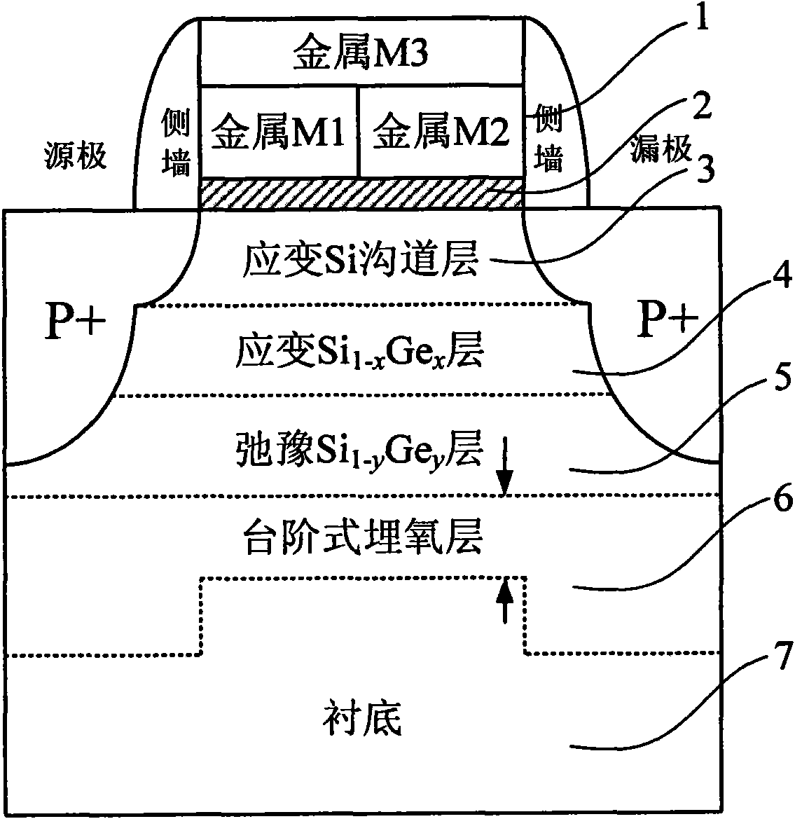
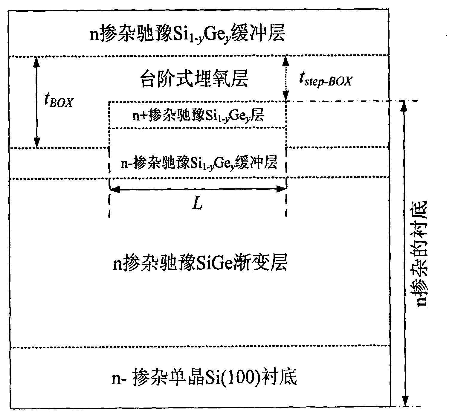
[0038] Such as figure 1 As shown, the heterogeneous metal stack gate SSGOI pMOSFET device structure of the present invention includes: a heterogeneous metal stack gate structure 1; gate insulating layer 2; intrinsic or n - Doped strained Si channel layer 3; intrinsic or n - Strained Si with Gradient Doping Composition 1-x Ge x Layer 4; n-doped relaxed Si 1-y Ge y layer 5; stepped buried oxide layer 6; n-doped substrate portion 7, ref. image 3 , the n-doped substrate part 7 is a thin layer (5-10 nanometers) of n + doped relaxed Si 1-y Ge y layer, n - doped relaxed Si 1-y Ge y buffer layer, n-doped relaxed SiGe graded layer and n - The doped single crystal Si (100) substrate consists of four parts.

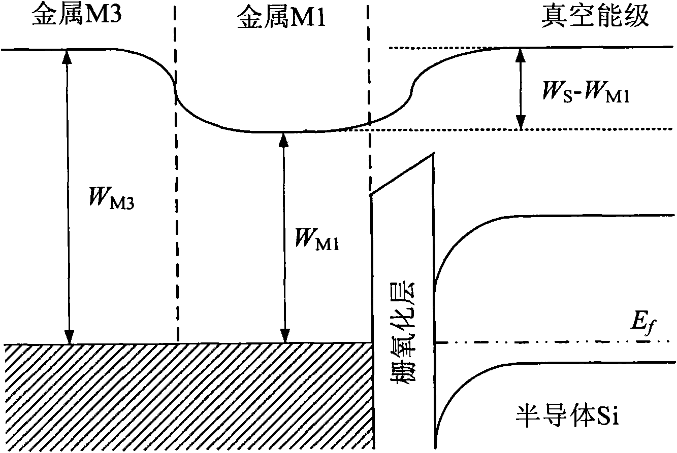
[0039] The heterogeneous metal stack gate structure includes a metal gate M1 near the source end, a metal gate M2 near the drain end, and a metal gate M3 above M1 and M2. M1 and M2 are completely covered by M3, and the work function W of the gate M1 M1 and the work f...


PUM


Abstract

The invention discloses a heterogeneous metal stacked grid strained silicon-germanium on insulator p-channel metal oxide semiconductor field effect tube (SSGOI pMOSFET) device structure, which comprises a heterogeneous metal stacked grid structure, a grid insulation layer, an intrinsic or n-doped strained Si channel layer, a strained Si1-xGex layer of which an intrinsic or n-doped component is changed gradually, an n-doped relaxation Si1-yGey layer, a stepped oxygen buried layer and an n-doped substrate part sequentially from top to bottom, wherein the n-doped substrate part consists of four parts, namely an n<+>-doped relaxation Si1-yGey layer, an n<->-doped relaxation Si1-yGey buffer layer, an n-doped relaxation SiGe gradient layer and an n<->-doped monocrystal Si(100) substrate. The device has a simple structure, can be totally compatible with the conventional Si silicon on insulator (SOI) process, is integrated with the advantages of grid engineering, strain engineering and substrate engineering, and makes a complementary metal-oxide-semiconductor structure process simply integrated.

Description

technical field [0001] The invention relates to a semiconductor MOSFET device structure in the field of microelectronics, in particular to a heterogeneous metal stack gate SSGOI pMOSFET device structure. Background technique [0002] With the continuous reduction of the characteristic length of modern semiconductor devices, their development is more and more restricted by physical limits, and the demand for high-speed and high-performance devices is becoming more and more intense. At this time, improving carrier mobility has become an effective strategy. means. At present, many obstacles are encountered in reducing the feature size of traditional silicon processes, and various secondary physical effects continue to appear. In order to continue the prediction of Moore's Law, the improvement of device structure and the introduction of new materials may play an important role in promoting the improvement of device characteristics, so the design and research of new materials an...

Claims


Application Information

Patent Timeline
IPC IPC(8): H01L29/78H01L29/49H01L29/06
Inventor 宋建军王冠宇张鹤鸣胡辉勇宣荣喜周春宇
Owner XIDIAN UNIV
Why Eureka
Try Eureka