Semiconductor light sources with doping gradients in optical confinement layers for improved device efficiency

a technology of semiconductor diodes and light sources, applied in semiconductor lasers, laser cooling arrangements, laser details, etc., can solve the problems of difficult to make single frequency lasers of the dfb type, limited dfb lasers designed to operate at shorter wavelengths, and suffer dbr devices, etc., to achieve high-efficiency conversion of electrical power into light energy

Active Publication Date: 2005-06-14
WISCONSIN ALUMNI RES FOUND
View PDF5 Cites 14 Cited by
  • Summary
  • Abstract
  • Description
  • Claims
  • Application Information

AI Technical Summary

Benefits of technology

[0009]The presence of a region of p-type doping in the confinement layer between the p-type cladding layer and the active region, which provides an electric field directed toward the active region, increases the transport speed of the injected holes toward the active region, thereby reducing the non-ohmic voltage drop and increasing the overall efficiency of the light emitting source. An n-type doped region may also be provided in the confinement layer between the n-type cladding layer and the active region. The doping in the confinement layer is formed to provide an electric field that is directed from the active region toward the n-type cladding layer, thereby increasing the speed of transport of electrons toward the active region, reducing the non-ohmic voltage drop, and increasing overall efficiency.
[0010]It is found in accordance with the invention that doping optical confinement layers in this manner significantly increases the carrier (holes or electrons) transport speed without significant losses due to free-carrier absorption where the confinement layers are substantially aluminum-free. Suitable aluminum-free semiconductor materials include InGaAsP, InGaP, and GaAs.

Problems solved by technology

A limitation is encountered with DFB lasers designed to operate at shorter wavelengths, including visible light wavelengths, in that conventional diode lasers grown on GaAs substrates, which can emit in the range of wavelengths between about 0.6 μm to 1.1 μm, generally have optical confinement layers next to the active region that contain aluminum, as well as cladding layers containing aluminum.
Due to the high reactivity of aluminum (i.e., essentially instant oxidation when exposed to air), it has proven to be very difficult to make single frequency lasers of the DFB type in the foregoing wavelength range in which the grating is buried within the multi-layer semiconductor structure.
However, such DBR devices suffer from the major drawback of mode hopping that occurs with increasing drive current due to changes in the lasing-region index of refraction with increasing drive power.
Another problem is encountered in SCH structures when the quantum-well active region is placed close to the n-doped cladding layer.
In a diode laser having an asymmetric type structure, low mobility injected holes from the p-doped cladding layer which have a small diffusion length can result in poor overall injection efficiency.

Method used


Image

  • Semiconductor light sources with doping gradients in optical confinement layers for improved device efficiency
  • Semiconductor light sources with doping gradients in optical confinement layers for improved device efficiency
  • Semiconductor light sources with doping gradients in optical confinement layers for improved device efficiency

Examples


Embodiment Construction

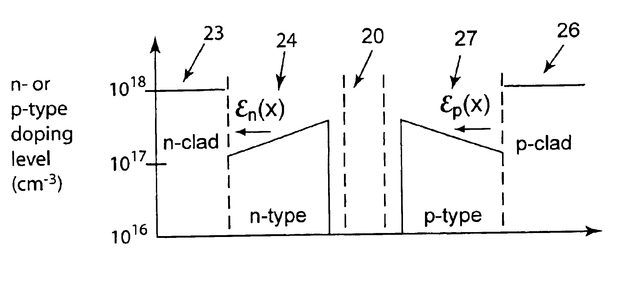
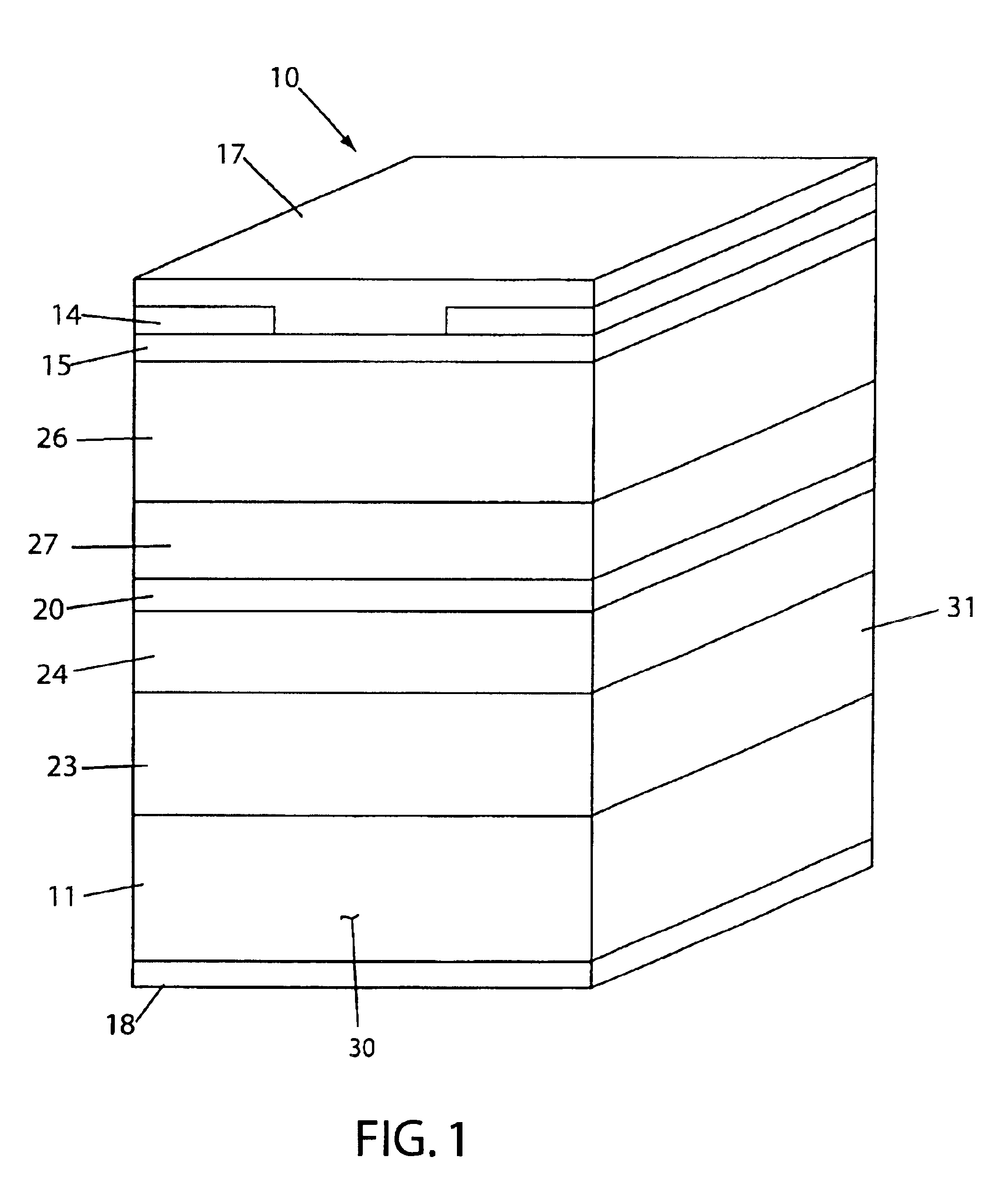
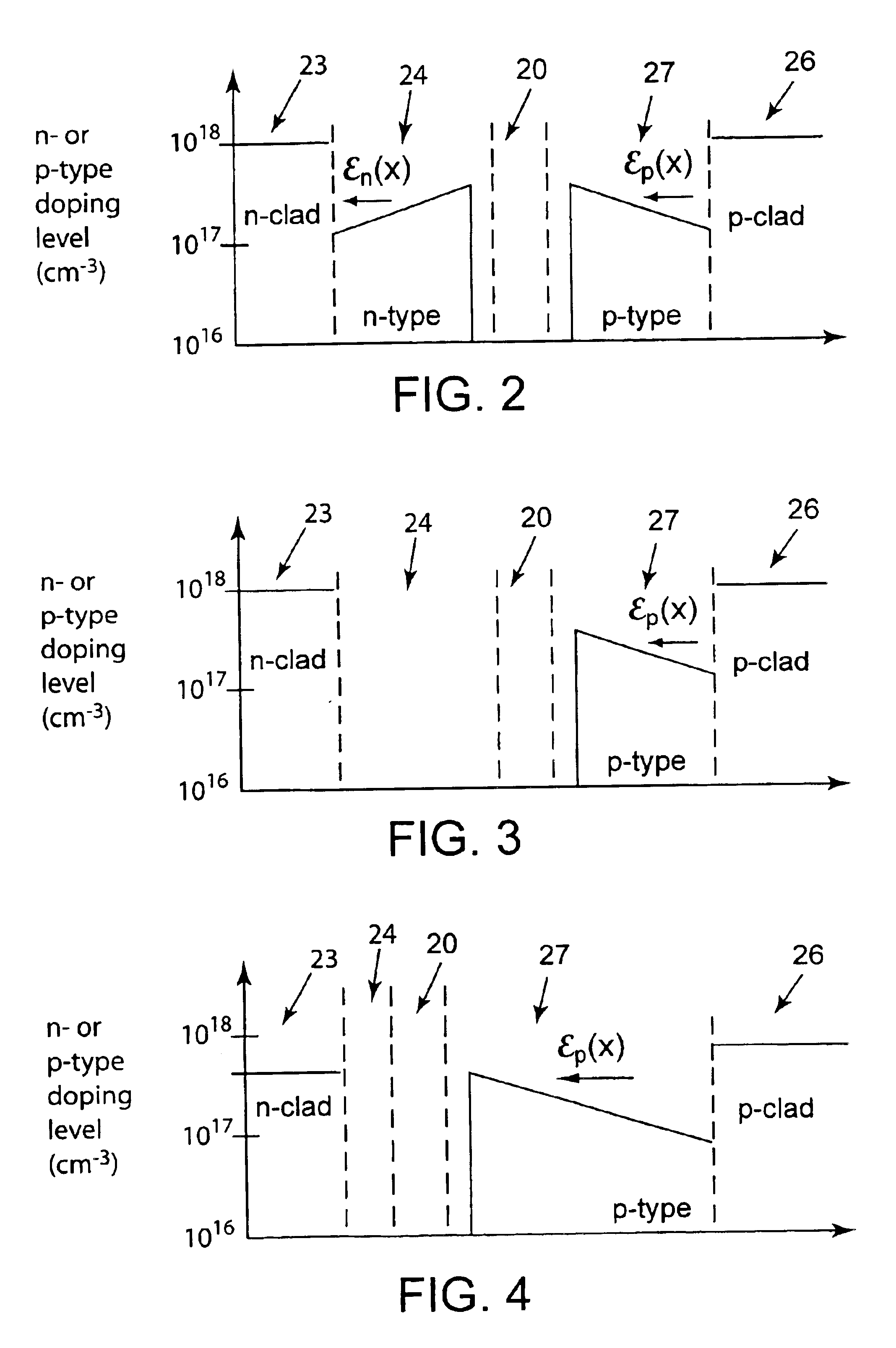
[0020]With reference to the drawings, a simplified view of a semiconductor laser incorporating the light source of the invention is shown generally at 10 in FIG. 1. It is understood that the exemplary semiconductor laser of FIG. 1 is provided for purposes of illustrating the invention and that the laser light source of the invention may be utilized in other laser structures or LEDs. The layers illustrated in FIG. 1 are epitaxially grown on a (preferably) GaAs substrate 11. The top surface of the substrate may be the (100) surface and the epitaxial layers may be grown on the surface exactly on orientation. Current confinement may be provided in various manners. For purposes of illustration only, current confinement can be provided as in FIG. 1 by defining the emitting aperture by insulating layers 14 (e.g., of SiO2) over a cap layer 15 of p+GaAs, with a top metal electrode 17 in contact with the cap layer at the top face between the insulating layer 14 to provide electrical conductio...


PUM


Abstract

Semiconductor light emitting sources are formed to have a substrate, an active region layer having one or more quantum wells, optical confinement layers surrounding the active region layer, and a p-type cladding layer and an n-type cladding layer surrounding the confinement layers and the active region layer. At least one of the optical confinement layers has a region of doping therein that is formed to provide a built-in electric field in the confinement layer that is directed to cause drift of carriers toward the active region. The electric field increases the transport speed of the injected holes or electrons, thereby reducing the non-ohmic voltage drop and increasing the overall efficiency of the light emitting source.

Description

FIELD OF THE INVENTION[0001]This invention pertains generally to the field of semiconductor diode lasers and amplifiers.BACKGROUND OF THE INVENTION[0002]Semiconductor diode lasers are formed of multiple layers of semiconductor materials. The typical semiconductor diode laser includes an n-type layer, a p-type layer and an undoped active region layer between them such that when the diode is forward biased electrons and holes recombine in the active region layer with the resulting emission of light. The layers surrounding the active layer typically have a lower index of refraction than the active layer and form cladding layers that confine the emitted light to the active layer and sometimes to adjacent layers. Semiconductor lasers may be constructed to be either edge emitting or surface emitting. In an edge emitting Fabry-Perot type semiconductor laser, crystal facet mirrors are located at opposite edges of the multi-layer structure to provide reflection of the emitted light back and ...

Claims


Application Information

Patent Timeline
Patent Type & Authority Patents(United States)
IPC IPC(8): H01S5/00H01S5/22
CPCH01S5/22H01S5/2226H01S5/2222
Inventor BOTEZ, DAN
Owner WISCONSIN ALUMNI RES FOUND
Why Eureka
Try Eureka