Class AB enhanced transconductance source follower

a source follower and transconductance technology, applied in the direction of amplifiers with semiconductor devices only, amplifiers with semiconductor devices, amplifiers, etc., can solve the problems of limiting the ability of source followers to drive loads, amplifiers with large quiescent currents are inherently energy inefficient, and traditional source followers also have the limitation of class a amplifiers, etc., to achieve enhanced transconductance source followers and low voltage high bandwidth

Active Publication Date: 2006-12-19
AVAGO TECH INT SALES PTE LTD
View PDF6 Cites 13 Cited by
  • Summary
  • Abstract
  • Description
  • Claims
  • Application Information

AI Technical Summary

Benefits of technology

[0007]The current invention is a low voltage, high bandwidth, enhanced transconductance source follower circuit constructed from Metal Oxide Silicon Field Effect Transistors (MOSFET) devices, which operates in a class AB mode. The class AB mode operation allows significantly more than the quiescent current to be available for both sourcing and sinking the output, resulting in significantly reduced average power consumption when driving the same load. Moreover, both the enhanced transconductance and the class AB mode operation of this invention are achieved while maintaining the large bandwidth of traditional source follower designs. The circuit of this invention can be used in a variety of applications, including voltage regulators and current conveyors

Problems solved by technology

However, traditionally designed source followers have relatively low transconductance, which limits their ability to drive loads, especially in modern, low voltage IC design.
Traditional source followers also have the limitation that they are class A type amplifiers, with a maximum load current limited to the quiescent current in the buffer.
Having a type A amplifier with large quiescent current is inherently energy inefficient.
Moreover, such circuits are limited in drive capability in one direction by the quiescent current.

Method used


Image

  • Class AB enhanced transconductance source follower
  • Class AB enhanced transconductance source follower
  • Class AB enhanced transconductance source follower

Examples


Embodiment Construction

[0016]During the course of this description like numbers will be used to identify like elements according to the different views that illustrate the invention.

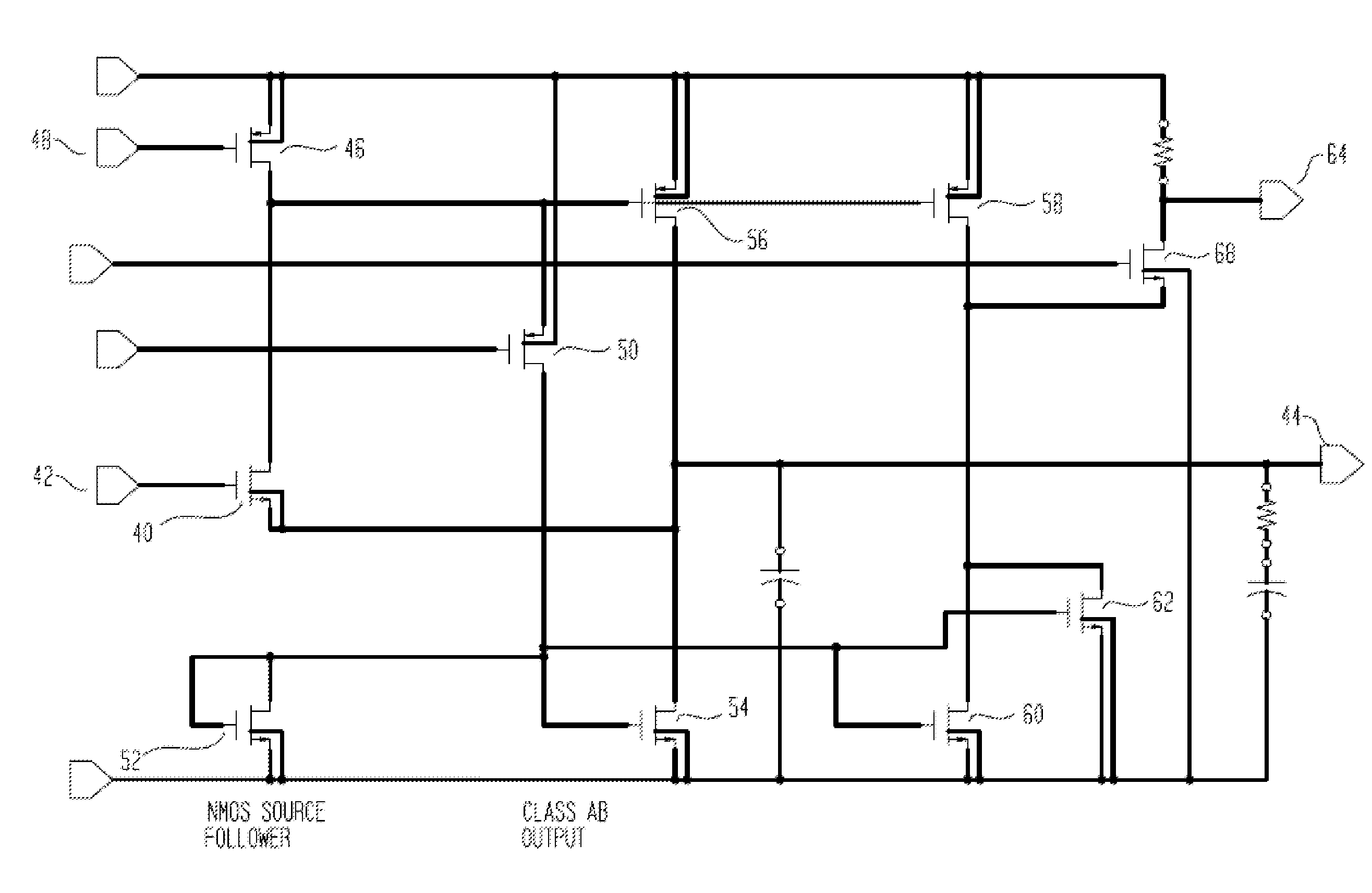
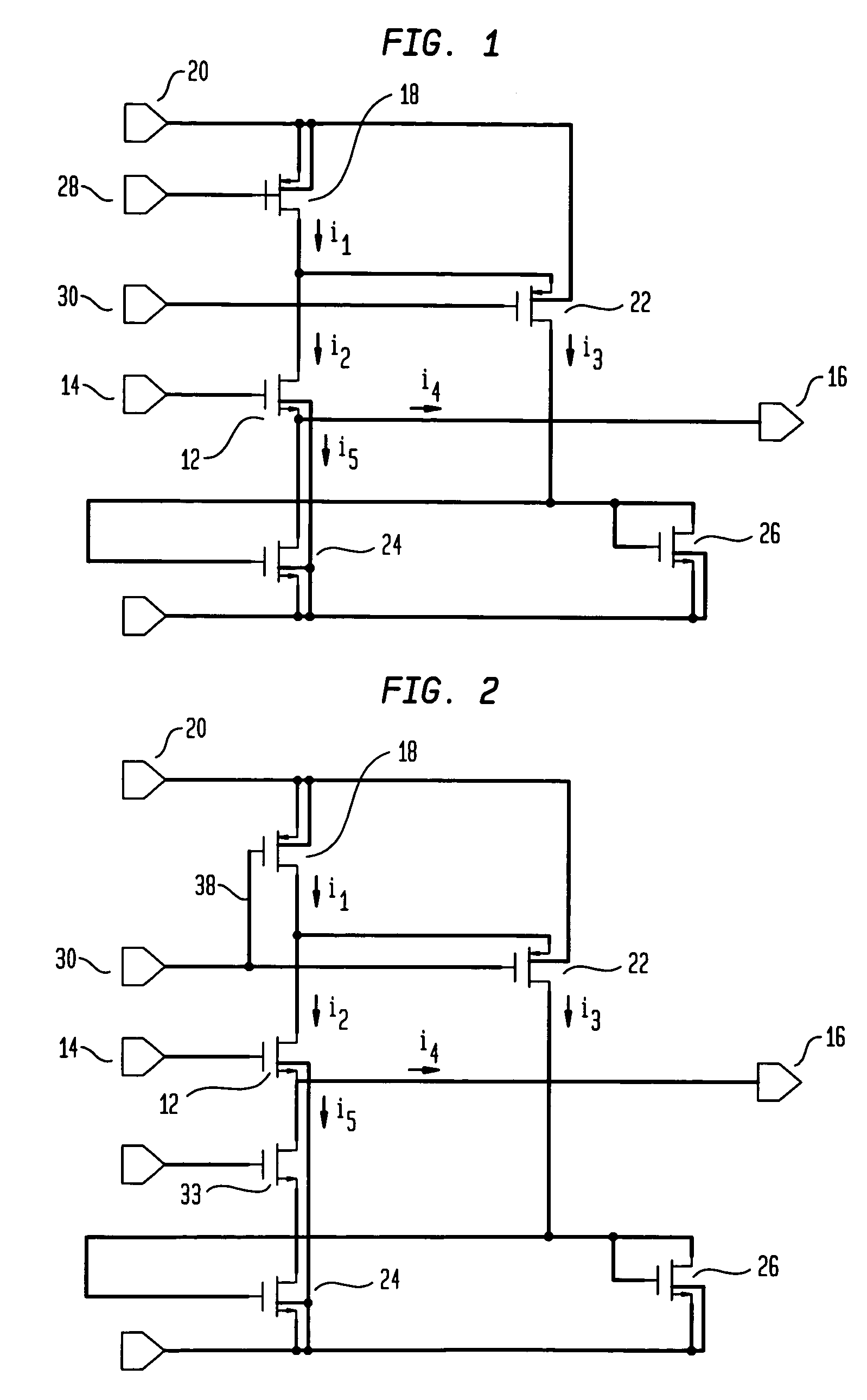
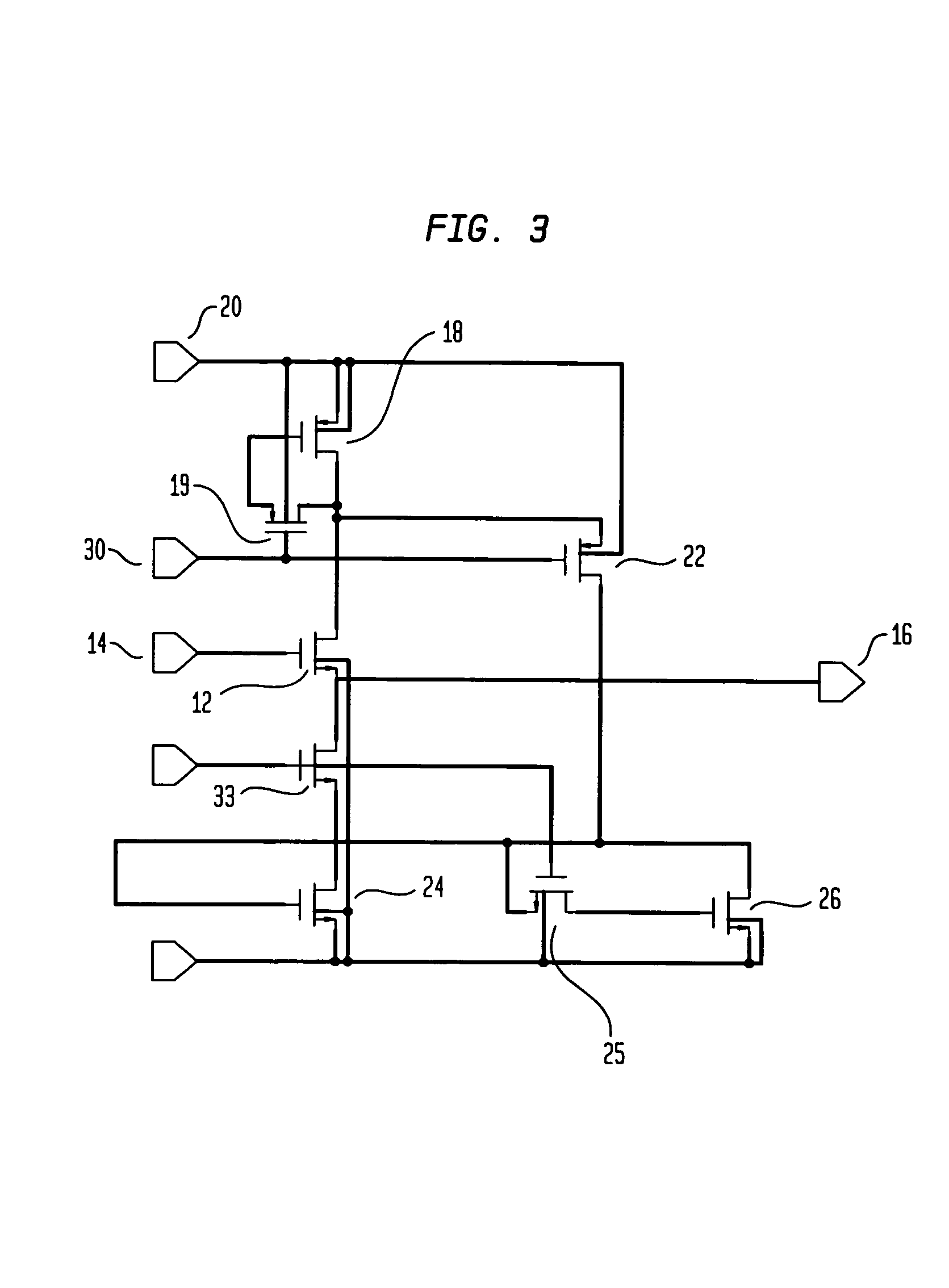
[0017]FIG. 1 is a schematic drawing of an enhanced transconductance source follower having class A behavior. Class A type amplifiers are limited to a maximum current output equal to the quiescent current, which makes their average power consumption very high. The class A type circuit of FIG. 1 provides a reference point for understanding the implementation and functioning of class AB circuits in accordance with this invention, as shown in FIGS. 2–6.

[0018]The circuit of FIG. 1 includes an NMOS source follower, transistor 12, having an input signal applied to its gate, or control terminal, at 13, and its source, a current flow terminal, is coupled to the output at 16. The circuit also has a current source, or supply, comprising the PMOS transistor 18. The drain, another current flow terminal, of PMOS 18 is connected to the rail ...


PUM


Abstract

A low voltage, high bandwidth, enhanced transconductance, source follower circuit constructed from MOS FET devices, which operates in a class AB mode. The drain current of the source follower is sensed with a folded cascode device. The sensed current is multiplied by a common source device of same type (NMOS or PMOS) as the source follower, and directed to the output load. Over limit current load at the source follower drain is sensed by a common source device of the opposite type (NMOS or PMOS), which also supplies the necessary extra current to the output load. This allows the device to supply significantly more than the quiescent current in both sourcing and sinking the output. Average power consumption for driving a given load is significantly reduced, while maintaining the large bandwidth of traditional source follower designs, and the capability for use in either voltage regulators or in a current conveyor.

Description

FIELD OF THE INVENTION[0001]The present invention relates to high bandwidth, high transconductance electronic integrated circuits, and particularly to high bandwidth, high transconductance source follower amplifiers having class AB operation characteristics.BACKGROUND OF THE INVENTION[0002]High frequency electronic integrated circuits (IC) used in modem electronic communications and computing devices require high bandwidth amplifiers. Furthermore, the low voltages used in modem IC designs lead to a need for high bandwidth amplifiers having a high transconductance, that is, amplifiers capable of generating significant change in output current for a relatively small change in input voltage. Such devices ideally should also have high input impedance and a choice of high or low output impedance. And, because modem electronic devices are increasingly portable, battery-powered devices, it is also highly desirous that the high bandwidth amplifiers be as energy efficient as possible.[0003]T...

Claims


Application Information

Patent Timeline
Patent Type & Authority Patents(United States)
IPC IPC(8): H03F3/18
CPCH03F1/0205H03F1/523H03F3/505H03F2200/462H03F2203/5012
Inventor FRANCK, STEPHEN J.JALALEDDINE, SATEH M.
Owner AVAGO TECH INT SALES PTE LTD
Why Eureka
Try Eureka