Nonvolatile latch circuit and logic circuit, and semiconductor device using the same

a logic circuit and nonvolatile technology, applied in the field of nonvolatile latch circuits and logic circuits, can solve the problems of large influence of variation in the amount of charge, inability to read circuits with high accuracy, and inability to reliably rewrite the number of rewrites and the reduction of voltage, etc., to achieve the effect of wide operating temperature range, low cost and low cos

Active Publication Date: 2011-08-04
SEMICON ENERGY LAB CO LTD
View PDF99 Cites 170 Cited by
  • Summary
  • Abstract
  • Description
  • Claims
  • Application Information

AI Technical Summary

Benefits of technology

[0022]In this manner, an embodiment of the present invention is to provide a nonvolatile latch circuit which has a wide operating temperature range and operates stably even at a high temperature and in which a logical state of storing data is not erased even after power is turned off.
[0038]According to an embodiment of the present invention, with the use of a transistor using an oxide semiconductor as a semiconductor material for forming a channel formation region, which serves as a switching element of a data holding portion, a nonvolatile latch circuit which has a wide operating temperature range and operates stably even at a high temperature and in which a logical state of storing data is not erased even after power is turned off, or a latch circuit provided with a data holding portion where a refresh period is sufficiently long can be realized. Since data writing is performed by switching of the transistor, the number of rewrites is not substantially limited. In addition, the writing voltage is almost equivalent to the threshold voltage of the transistor; thus, the data writing can be performed at a low voltage. Further, the charge accumulated in the capacitor of the data storing portion can be kept held as data without any change; therefore, the variation in the amount of charge which is stored as data can be suppressed small and data can be read easily as compared to the case where remanent polarization is used as data.
[0039]Various logic circuits can be provided by using the nonvolatile latch circuit. For example, in the logic circuit using the nonvolatile latch circuit, the power consumption can be reduced by turning off power of the unused block. In addition, since a logical state is stored even when power is turned off, a system can be started when power is turned on or terminated when power is turned off, at high speed and low power.

Problems solved by technology

However, a nonvolatile latch circuit using a ferroelectric element has problems in terms of reliability of the number of rewrites and reduction in voltage.
However, when the remanent polarization is small, the following problems might arise: the influence of variation in the amount of charge becomes large, and a high-accuracy reading circuit is needed.

Method used


Image

  • Nonvolatile latch circuit and logic circuit, and semiconductor device using the same
  • Nonvolatile latch circuit and logic circuit, and semiconductor device using the same
  • Nonvolatile latch circuit and logic circuit, and semiconductor device using the same

Examples


embodiment 1

[0072]In this embodiment, a configuration and an operation of a nonvolatile latch circuit which is an embodiment of the invention disclosed herein; and a structure, a manufacturing method, and the like of elements of the nonvolatile latch circuit will be described with reference to FIG. 1, FIGS. 2A and 2B, FIGS. 3A and 3B, FIGS. 4A to 4H, FIGS. 5A to 5G, FIGS. 6A to 6D, FIG. 7, FIG. 8, FIGS. 9A and 9B, FIG. 10, FIG. 11, FIG. 12, FIG. 13, FIG. 14, and FIG. 15.

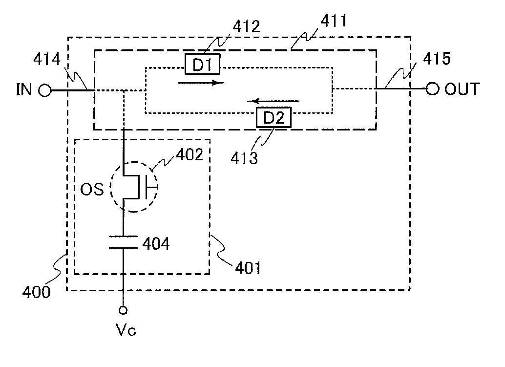
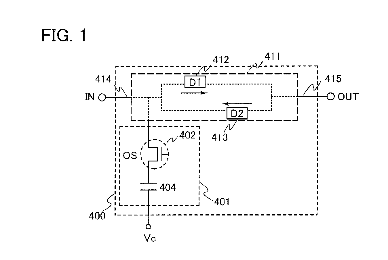
[0073]FIG. 1 illustrates a configuration of a nonvolatile latch circuit 400 including a latch portion 411 and a data holding portion 401 for holding data of the latch portion.

[0074]The nonvolatile latch circuit 400 in FIG. 1 includes the latch portion 411 having a loop structure and the data holding portion 401 for holding data of the latch portion. In the latch portion 411 having a loop structure, an output of a first element (D1) 412 is electrically connected to an input of a second element (D2) 413, and an output of the secon...

embodiment 2

[0246]In this embodiment, another example of a structure, a manufacturing method, and the like of elements of the nonvolatile latch circuit which is an embodiment of the invention disclosed herein will be described with reference to FIG. 16, FIGS. 17A to 17E, and FIGS. 18A to 18D. In this embodiment, the configuration of the nonvolatile latch circuit is similar to that in FIG. 1.

[0247]FIG. 16 is a cross-sectional view illustrating an example of structures of elements of a nonvolatile latch circuit. FIG. 16 is an example in which, among the elements of the nonvolatile latch circuit, the structure of a transistor 402 formed using an oxide semiconductor in the upper portion is different from that in FIGS. 3A and 3B. In other words, FIG. 16 is an example in which a top-gate transistor is applied to the transistor 402 formed using an oxide semiconductor in the upper portion. The structures of the other elements (the structure of the transistor in the lower portion, and the like) are simi...

embodiment 3

[0342]In this embodiment, the configuration and the operation of the nonvolatile latch circuit which is an embodiment of the invention disclosed herein will be described with reference to FIGS. 19A and 19B.

[0343]FIG. 19A illustrates a configuration of the nonvolatile latch circuit 400 including the latch portion 411 and the data holding portion 401 for holding data of the latch portion. FIG. 19B illustrates an example of a timing chart of the nonvolatile latch circuit 400.

[0344]FIG. 19A is an example in which the configuration of the latch portion 411 in FIG. 1 is specifically illustrated. FIG. 19A is an example of the configuration of the latch portion 411 in FIG. 1, where an inverter 412 is used for the first element and an inverter 413 is used for the second element. The structure of the transistor 402 can be similar to that in Embodiment 1 or Embodiment 2.

[0345]The latch portion 411 includes the inverter 412 and the inverter 413. The latch portion 411 has a loop structure in whi...


PUM


Abstract

To provide a novel nonvolatile latch circuit and a semiconductor device using the nonvolatile latch circuit, a nonvolatile latch circuit includes a latch portion having a loop structure where an output of a first element is electrically connected to an input of a second element, and an output of the second element is electrically connected to an input of the first element; and a data holding portion configured to hold data of the latch portion. In the data holding portion, a transistor using an oxide semiconductor as a semiconductor material for forming a channel formation region is used as a switching element. In addition, a capacitor electrically connected to a source electrode or a drain electrode of the transistor is included.

Description

TECHNICAL FIELD[0001]The invention disclosed herein relates to a nonvolatile logic circuit in which the logical state of storing data is not erased even after power is turned off, and a semiconductor device using the nonvolatile logic circuit. In particular, the invention disclosed herein relates to a nonvolatile latch circuit and a semiconductor device using the nonvolatile latch circuit.BACKGROUND ART[0002]An integrated circuit has been proposed in which nonvolatile logic is integrated, where a feature of “nonvolatile” with which data is not erased even when power is turned off is applied to a logic circuit. For example, a nonvolatile latch circuit using a ferroelectric element as nonvolatile logic has been proposed (see Patent Document 1).REFERENCEPatent Document[0003][Patent Document 1] PCT International Publication No. 2003 / 044953DISCLOSURE OF INVENTION[0004]However, a nonvolatile latch circuit using a ferroelectric element has problems in terms of reliability of the number of ...

Claims


Application Information

Patent Timeline
Patent Type & Authority Applications(United States)
IPC IPC(8): H03K19/173G11C11/24
CPCG11C14/0054H01L27/0688H03K19/173H01L27/1225G11C11/24H01L27/105H01L27/1207H01L27/1255H01L29/045H01L29/7869H03K3/037
Inventor KATO, KIYOSHIKOYAMA, JUN
Owner SEMICON ENERGY LAB CO LTD
Why Eureka
Try Eureka