Group III-nitride semiconductor device with a cap layer

a technology of nitride and semiconductor, applied in the direction of semiconductor/solid-state device manufacturing, semiconductor devices, semiconductor devices, etc., can solve the problems of insufficient source resistance in the conventional semiconductor device, reduce the source resistance to achieve higher high frequency characteristics, and achieve the effect of reducing the source resistance, enhancing the transconductance of the transistor, and achieving higher high frequency band

Active Publication Date: 2010-09-21
PANASONIC CORP
View PDF8 Cites 15 Cited by
  • Summary
  • Abstract
  • Description
  • Claims
  • Application Information

AI Technical Summary

Benefits of technology

[0013]The present invention has its object of reducing the source resistance while enhancing the transconductance of a transistor made of a group III nitride semiconductor by solving the conventional problems and the newly-found problems.

Problems solved by technology

This reduces the source resistance to attain higher high frequency characteristics.
The above conventional semiconductor device composed of a MIS type HFET, however, involves the following problems.
This means that the source resistance is reduced insufficiently in the conventional semiconductor device.

Method used


Image

  • Group III-nitride semiconductor device with a cap layer
  • Group III-nitride semiconductor device with a cap layer
  • Group III-nitride semiconductor device with a cap layer

Examples


embodiment 1

[0065]Embodiment 1 of the present invention will now be described with reference to the accompanying drawings.

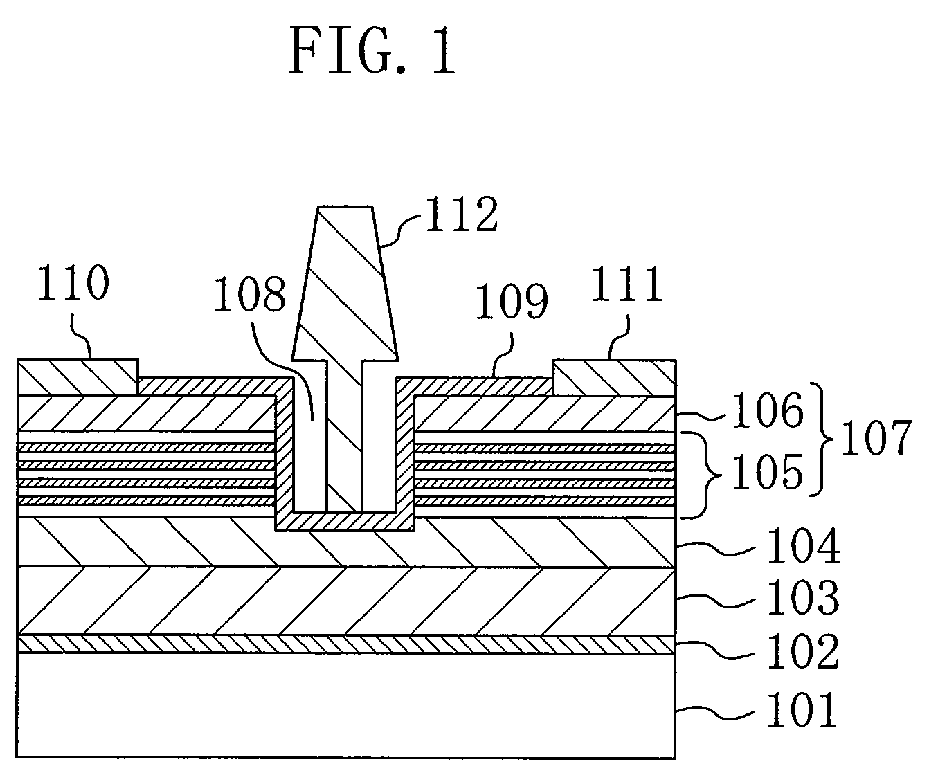
[0066]FIG. 1 shows a sectional structure of a MIS type HFET as a semiconductor device in accordance with Embodiment 1 of the present invention.

[0067]As shown in FIG. 1, a buffer layer 102, an active layer 103, a barrier layer 104, a superlattice layer 105, and an n-type GaN layer 106 are formed in this order on the principal face of a substrate 101 made of sapphire (single crystal of Al2O3) by epitaxial growth. The buffer layer 102 is made of aluminum nitride (AlN) or gallium nitride (GaN) grown at low temperature. The active layer 103 is made of GaN. The barrier layer 104 is made of aluminum gallium nitride (Al0.26Ga0.74N). The superlattice layer 105 is formed by layering an n-type Al0.26Ga0.74N layer with a thickness of 5.6 nm and an n-type GaN layer with a thickness of 1.4 nm seven times. The n-type GaN layer 106 has a thickness of 20 nm. A combination of the superlattice...

embodiment 2

[0084]Embodiment 2 of the present invention will be described below with reference to the drawings.

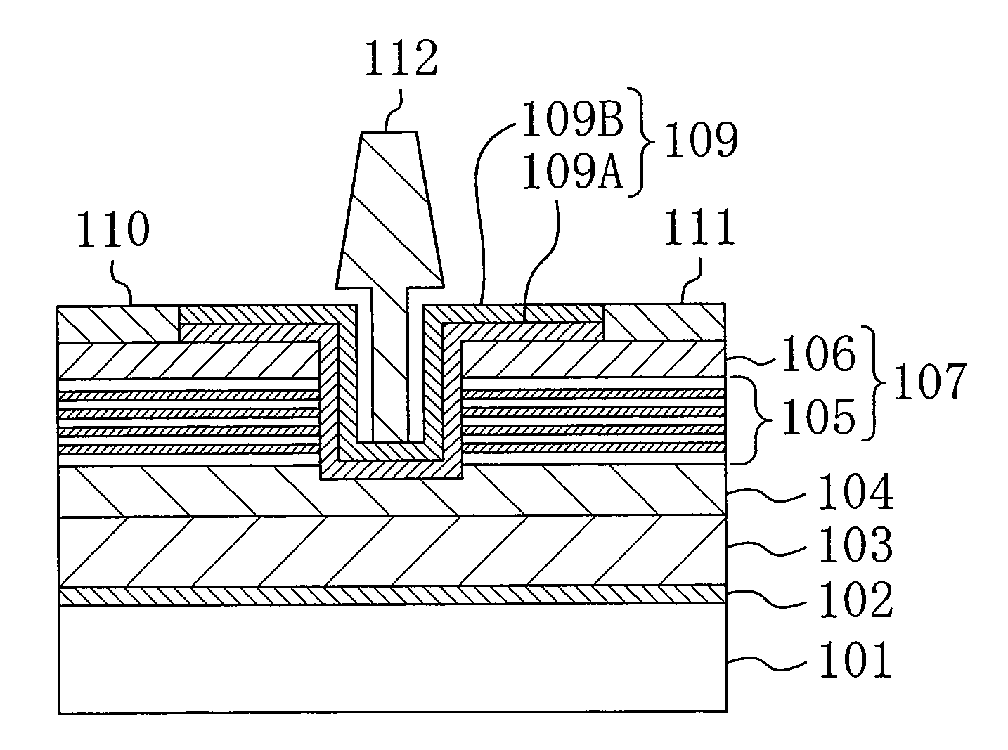
[0085]FIG. 6 shows a sectional structure of a MIS-type HFET as a semiconductor device according to Embodiment 2 of the present invention. In FIG. 6, the same reference numerals are assigned to the same elements as those shown in FIG. 1 for omitting description thereof.

[0086]As shown in FIG. 6, in the semiconductor device of Embodiment 2, the insulating film 109 formed between the gate electrode 112 and the barrier layer 104 is formed of a lower insulating film 109A formed by MOCVD, for example, and made of silicon nitride (SiN) with a thickness of approximately 3 nm and an upper insulating film 109B formed by p-CVD, for example, and made of silicon nitride (SiN) with a thickness of approximately 4 nm.

[0087]The two-layer structure of the insulating film 109 as a gate insulating film exhibits the following effect.

[0088]Namely, the insulating property of the insulating film 109 is enhance...

embodiment 3

[0092]Embodiment 3 of the present invention will be described below with reference to the drawings.

[0093]FIG. 8 shows a sectional structure of a MIS-type HFET as a semiconductor device in accordance with Embodiment 3 of the present invention. In FIG. 8, the same reference numerals are assigned to the same elements as those shown in FIG. 6 for omitting description thereof.

[0094]As shown in FIG. 8, in the semiconductor device of Embodiment 3, a concave part 109b for exposing the lower insulating film 109A is formed at the bottom of the gate recess 108 in the upper insulating film 109B forming the insulating film 109. A lower end portion 112a of the gate electrode 112 is filled in the concave part 109b formed in the upper insulating film 109B. Wherein, the opening width in the gate length direction of the concave part 109b is smaller than the width of a part of the gate electrode 112 which is located on the upper insulating film 109B.

[0095]With the above structure, a part of the insula...


PUM


Abstract

A semiconductor device includes: a first semiconductor layer which is made of a first group III nitride semiconductor; a cap layer which is formed on the first semiconductor layer, which is made of a second group III nitride semiconductor, and which has an opening for exposing the first semiconductor layer; and a source electrode and a drain electrode which are formed on the cap layer so as to oppose to each other with the opening interposed. A gate electrode is formed on the bottom face of the opening with an insulating film interposed. The insulating film is formed on at least a part of the first semiconductor layer which is exposed through the opening.

Description

CROSS REFERENCE TO RELATED APPLICATIONS[0001]This non-provisional application claims priority under 35 U.S.C. §119(a) on Patent Application No. 2007-087370 filed in Japan on Mar. 29, 2007, the entire contents of which are hereby incorporated by reference.BACKGROUND OF THE INVENTION[0002]The present invention relates to a semiconductor device made of a group III nitride semiconductor and a method for manufacturing it, and particularly relates to a semiconductor device including a MIS (metal insulator semiconductor) type gate electrode and a method for manufacturing it.[0003]Group III nitride semiconductors, which are typified by nitride gallium (GaN), as a mixed crystal expressed by a general formula of (InxAl1-x)yGa1-yN (wherein x and y are in the ranges of 0≦x≦1, 0≦y≦1, and 0≦x+y≦1), are expected to be applied not only to visible or ultraviolet light emitting elements utilizing a physical characteristic of wide bandgap and a direct transition band structure but also to electronic d...

Claims


Application Information

Patent Timeline
Patent Type & Authority Patents(United States)
IPC IPC(8): H01L31/0256
CPCH01L29/155H01L29/432H01L29/66462H01L29/7786H01L29/2003H01L29/4175H01L29/513
Inventor MURATA, TOMOHIROKURODA, MASAYUKIUEDA, TETSUZO
Owner PANASONIC CORP
Why Eureka
Try Eureka