Nanowire based vertical circular grating transistor and preparation method thereof

A nanowire and transistor technology, applied in the field of nanoelectronics, achieves the effects of improving transconductance, suppressing short-channel effect, and reducing parasitic resistance

Inactive Publication Date: 2014-01-22
PEKING UNIV
View PDF3 Cites 16 Cited by
  • Summary
  • Abstract
  • Description
  • Claims
  • Application Information

AI Technical Summary

Problems solved by technology

However, in the device structure of this article, there is an unregulated nanowire between the source and the gate, and between the gate and the drain. This nanowire introduces a parasitic resistance that has a great influence and inhibits the RF performance of the device. promotion

Method used


Image

  • Nanowire based vertical circular grating transistor and preparation method thereof
  • Nanowire based vertical circular grating transistor and preparation method thereof
  • Nanowire based vertical circular grating transistor and preparation method thereof

Examples


Embodiment Construction

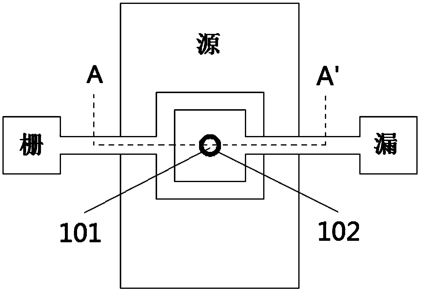
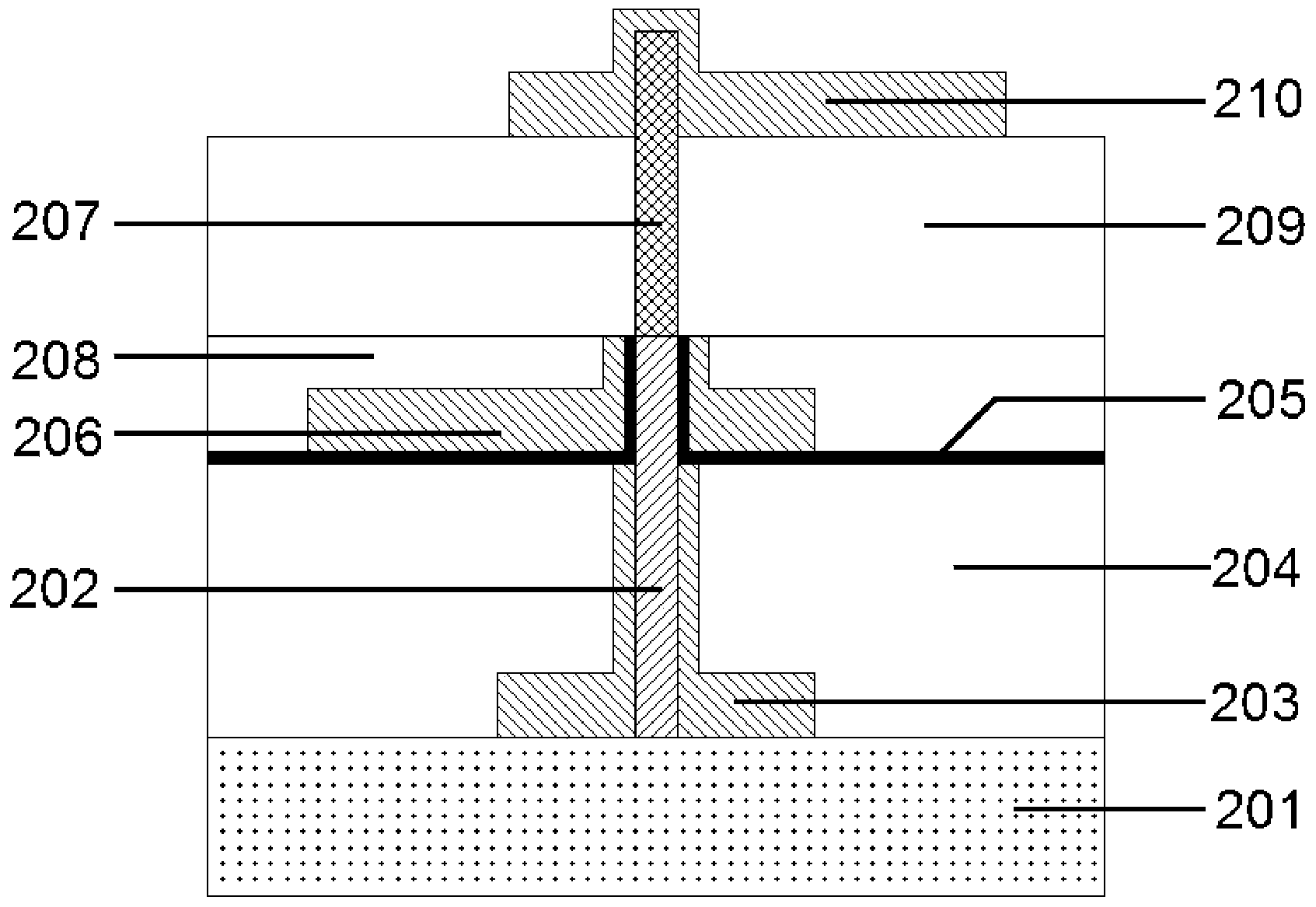
[0046] In the following, the present invention will be further described in detail by taking a vertical gate-around transistor based on InAs nanowires as an example in conjunction with the accompanying drawings.

[0047] figure 1 is a schematic top view of the embodiment transistor, figure 2 is along figure 1 The cross-sectional schematic diagram of A-A' direction in the figure. The substrate can be single crystal silicon or single crystal silicon covered with a layer of silicon oxide, the intrinsic or low-doped InAs nanowires are perpendicular to the substrate surface, and there is no gap on the intrinsic or low-doped InAs nanowires The low-resistance nanowires are connected. The low-resistance nanowires can be heavily doped InAs nanowires or InAs-metal alloy nanowires. The intrinsic or low-doped InAs nanowires are respectively source electrodes, The gate dielectric and the gate electrode are surrounded by the low-resistance nanowire from bottom to top and are respectivel...


PUM


Abstract

The invention discloses a nanowire based vertical circular grating transistor and a preparation method thereof. According to the structure, a conducting channel material is an intrinsic or low doped nanowire perpendicular to a substrate; a low-resistance nanowire is connected above the intrinsic or low doped nanowire in a gapless manner; the intrinsic or low doped nanowire is surrounded by a source electrode, a gate medium and a gate electrode sequentially from bottom to top; the source electrode and the gate medium as well as the gate medium and the grate electrode are connected in the position of the side wall of the nanowire in a gapless manner; the low-resistance nanowire is surrounded by a drain electrode; and three isolation layers are arranged among the electrodes. The invention further provides the preparation method of the transistor. Both the source electrode and the gate electrode are obtained with the method that firstly, a metal film is plated and then metal above BCB (benzocyclobutene) is eroded by using BCB as a mask; and the low-resistance nanowire is obtained through heavy doping of the intrinsic or low doped nanowire or through metal alloy. According to the short-channel transistor structure and the preparation method, a device with a short channel can be prepared, the parasitic resistance and the parasitic capacitance can be effectively reduced, and the device performance is improved.

Description

technical field [0001] The invention belongs to the technical field of nanoelectronics, and in particular relates to a vertical gate-around transistor based on nanowires and a preparation method thereof. Background technique [0002] With the development of the semiconductor industry, the integration of chips is getting higher and higher, and the size of a single MOS device is getting smaller and smaller. Various problems caused by size reduction have begun to appear, one of which is the short-channel effect. In order to suppress the short-channel effect, various gate structures, such as SOI and FinFET, have been proposed. Among all the gate structures, the gate-around structure can greatly improve the ability of gate regulation and suppress the short channel effect. Compared with traditional bulk materials, one-dimensional materials such as nanowires have the natural advantage of being easy to prepare gate-all-around structures. [0003] Among semiconductor materials, the...

Claims


Application Information

Patent Timeline
Patent Type & Authority Applications(China)
IPC IPC(8): H01L29/78H01L29/423H01L21/336H01L21/28
CPCH01L29/42356H01L29/66666H01L29/7827
Inventor 史团伟陈清许胜勇徐洪起
Owner PEKING UNIV
Why Eureka
Try Eureka