Manufacturing method of transistor

A manufacturing method and transistor technology, which are applied in semiconductor/solid-state device manufacturing, semiconductor device, photoengraving process coating equipment, etc., can solve the problems of large discreteness and large parasitic elements, improve uniformity and reduce parasitic elements the effect of

Active Publication Date: 2011-07-20
BOE TECH GRP CO LTD
View PDF7 Cites 39 Cited by
  • Summary
  • Abstract
  • Description
  • Claims
  • Application Information

AI Technical Summary

Problems solved by technology

The non-self-aligned process will lead to large dispersion of device characteristics and large parasitic components (such as parasitic capacitance), which are unacceptable for flat panel display applications

Method used


Image

  • Manufacturing method of transistor
  • Manufacturing method of transistor
  • Manufacturing method of transistor

Examples


Embodiment Construction

[0032] Hereinafter, the present invention will be further described in detail through specific embodiments in conjunction with the drawings.

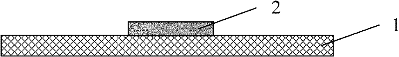
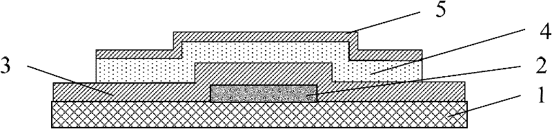
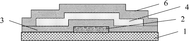
[0033] In the prior art, the process method of the double-gate structure of the thin film transistor determines that the top gate electrode and the bottom gate electrode cannot be accurately aligned, which results in a large parasitic capacitance of the transistor, which limits its performance. The present invention adopts an opaque design when fabricating the bottom gate electrode. For example, an opaque material can be used. When the substrate, the top gate electrode, and the layers between the bottom gate electrode and the top gate electrode are fabricated, a transparent design is adopted. The design of light characteristics, for example, can adopt light-transmitting materials or design the thickness to make it have light-transmitting characteristics; when the top gate electrode pattern is formed by photolithography, the bottom gate elec...


PUM


Abstract

The invention discloses a manufacturing method of a thin film transistor with a double gate structure. An active region of the transistor and a top gate electrode are made of a transparent thin film material. The manufacturing method comprises the following steps of: during photoetching coating, coating photoresist on the surface of a transparent conductive thin film of the top gate electrode; during photoetching exposure, carrying out exposure from the back surface of a substrate; after photoetching development, forming a photoetching diagram over against a bottom gate electrode on the surface of the conductive thin film; and etching the conductive thin film to form the top gate electrode over against the bottom gate electrode according to the photoetching diagram. The double gate thin film transistor formed by adopting the method adopts the bottom gate electrode as a natural mask plate, saves the manufacturing cost of the transistor, improves the alignment precision of the top gate electrode and the bottom gate electrode and enhances the performance of the double gate structure thin film transistor.

Description

Technical field [0001] The invention relates to the manufacture of transistors, in particular to a method for manufacturing a double-gate thin film transistor. Background technique [0002] Thin film transistors, as switch control components or integrated components of peripheral drive circuits, are one of the core devices in flat panel display technology, and their performance directly affects the effect of flat panel displays. The existing thin film transistors include single-gate structures and double-gate structures. Compared with thin film transistors of single-gate structure, the double-gate structure has the advantages of stronger driving capability, steeper sub-threshold slope, and significantly reduced circuit footprint. Moreover, the reasonable and clever use of the double-gate combination can realize new functional devices and circuits. However, the biggest problem of the double-gate structure thin film transistor, especially the planar double-gate, is the complicate...

Claims


Application Information

Patent Timeline
Patent Type & Authority Applications(China)
IPC IPC(8): H01L21/336H01L21/28G03F7/16G03F7/20
CPCH01L29/78648H01L29/66742H01L29/7869H01L29/66969
Inventor 张盛东贺鑫王龙彦
Owner BOE TECH GRP CO LTD
Why Eureka
Try Eureka