Power MOSFET

a power mosfet and lateral technology, applied in the field ofsemiconductor devices, can solve the problems of high on-state resistance of conventional lateral power mosfets, increase fabrication costs, and errors, and achieve the effect of reducing parasitic resistan

Inactive Publication Date: 2005-12-06
GREAT WALL SEMICON CORP
View PDF2 Cites 38 Cited by
  • Summary
  • Abstract
  • Description
  • Claims
  • Application Information

AI Technical Summary

Benefits of technology

[0009]The present invention discloses a system for interconnecting regions on a semiconductor substrate using wide metal runners or a planar interconnection layer, and a plurality of solder bumps on conductive pads arranged in a checkerboard pattern or interleaved, thereby reducing parasitic resistance. The interconnections may be used for connecting discrete as well as integrated devices.

Problems solved by technology

However, these conventional lateral power MOSFETs exhibit problems of high on-state resistance due to the parasitic resistance of metal interconnects.
This problem is exacerbated when the die size of the transistor is scaled up and a large number of transistor cells are connected in parallel to handle greater power loads.
The complexity of such a process increases the fabrication costs, errors, and also problems with latch-up.
Bipolar devices are also susceptible to the same problems as MOSFETs with high on-state resistance due to the parasitic resistance of the metal interconnects for similar reasons.

Method used


Image

  • Power MOSFET
  • Power MOSFET
  • Power MOSFET

Examples


Embodiment Construction

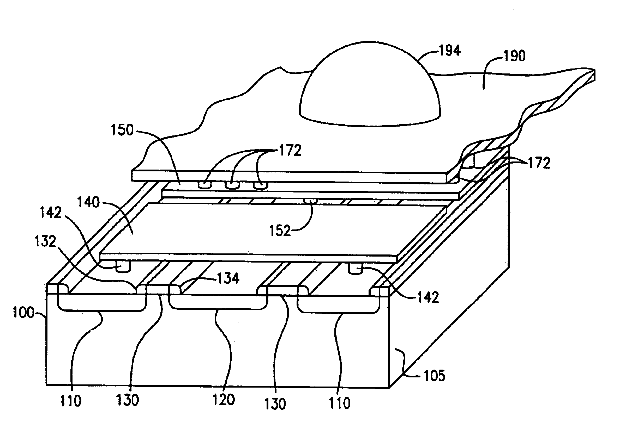
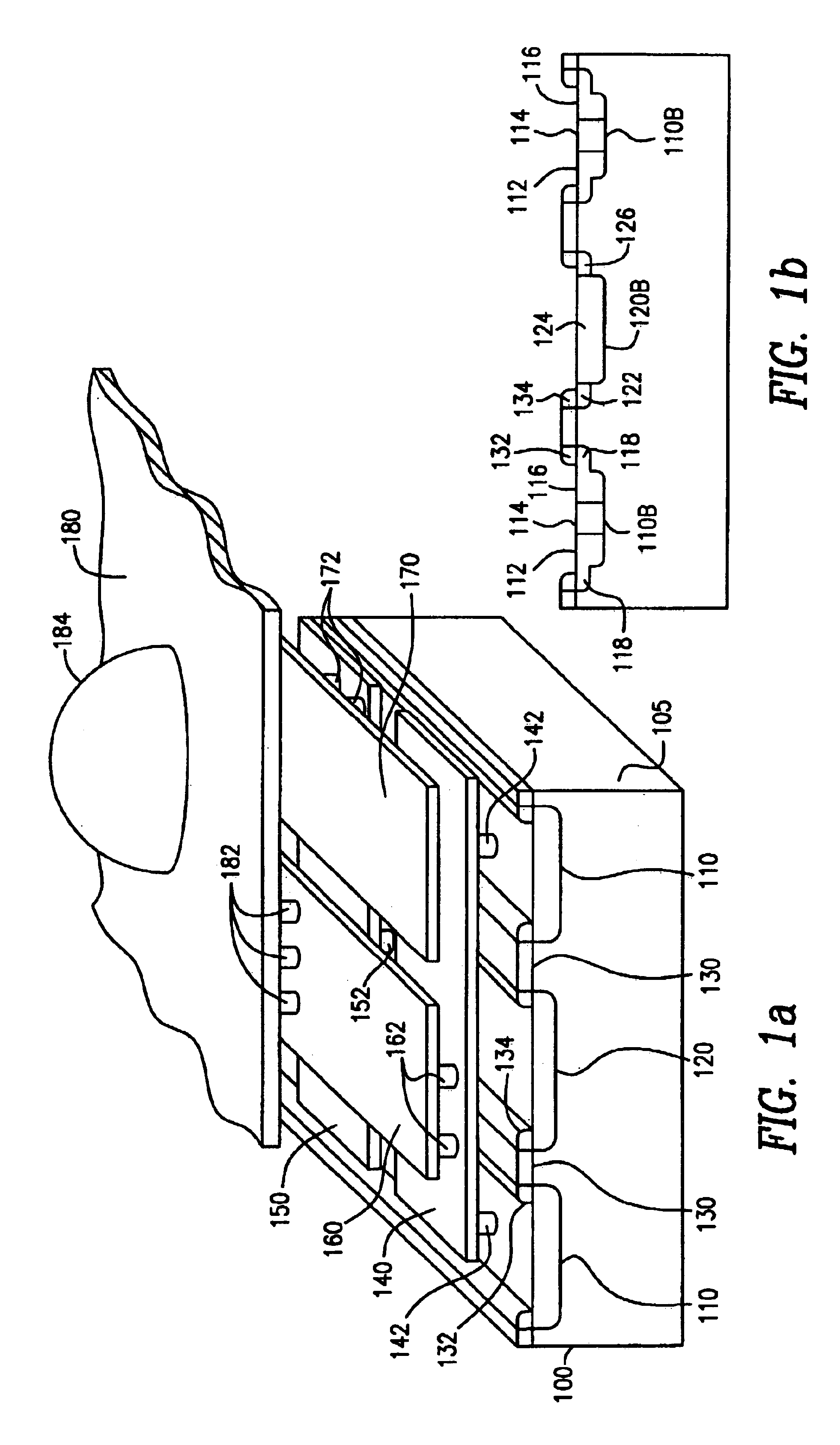
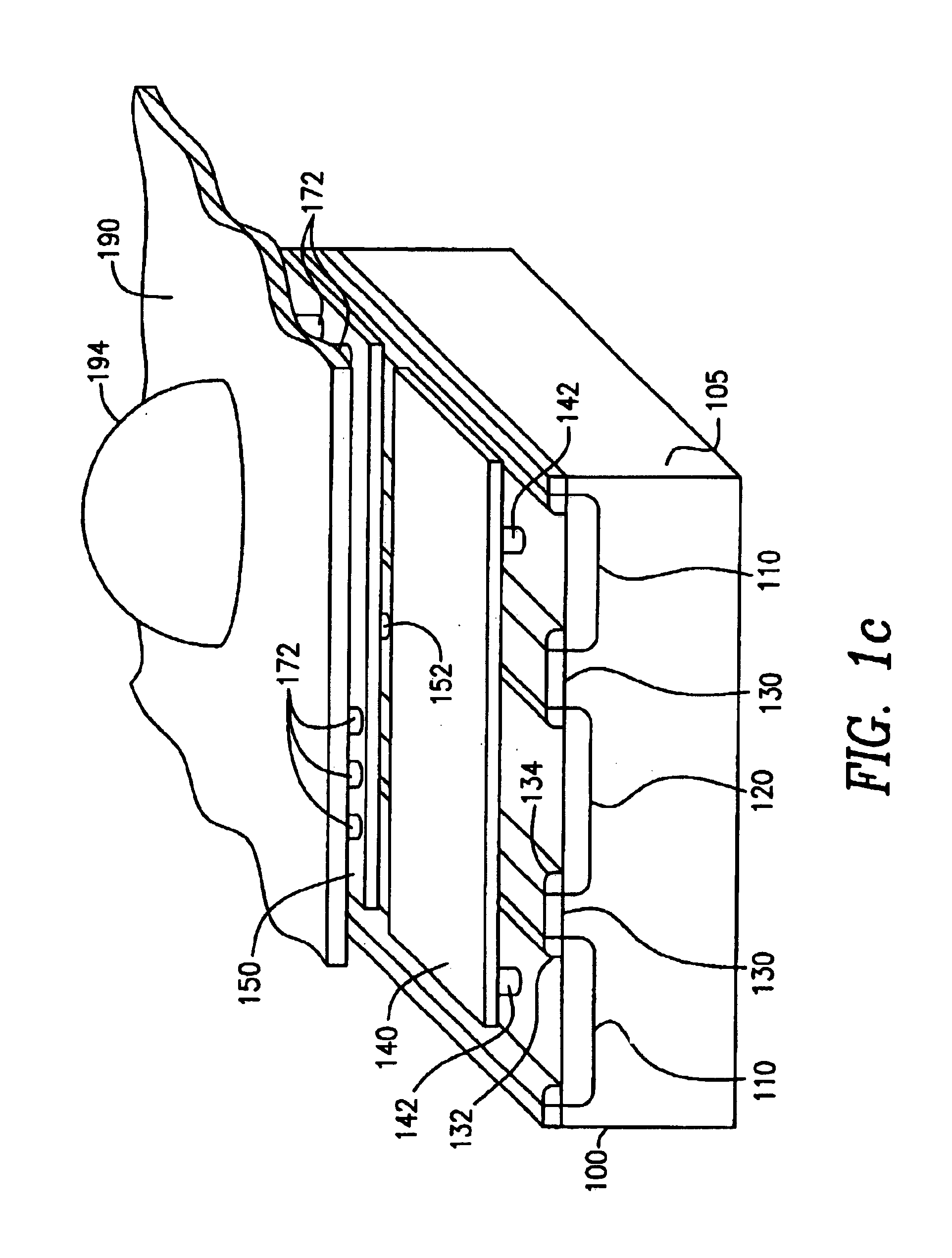
[0012]The preferred embodiment of the present invention uses conventional CMOS fabrication processes to fabricate a semiconductor device embodying the present invention to reduce the costs of production. In accordance with one aspect of the present invention, however, only one type of MOSFETs (either an n-channel or p-channel MOSFET) is made on the die. Since the device of the present invention only consists of parallel n-channel or p-channel transistors, the problem of latch-up is avoided.

[0013]In another preferred embodiment no field implants are used, although alternate embodiments may use field implants if there is more than one transistor on a die.

[0014]Yet further, in another preferred embodiment of the invention there is no local field oxide layer since the preferred embodiment is constructed having only one device per die.

[0015]Yet further, in another preferred embodiment of the invention a self-aligned silicide is formed over the source, drain and gate of the transistor.

[00...


PUM


Abstract

A system of interconnecting regions on an integrated semiconductor device or discrete components. As first connectivity layer has first and second runners to interconnect a plurality of first and second regions. A second connectivity layer has third runners to interconnect the first runners and fourth runners to interconnect the second runners. A third connectivity layer has first pads connected to the third runners and second pads connected to the fourth runners. Solder bumps are used on the first and second pads to connect the pads to other circuits.

Description

CROSS-REFERENCE TO RELATED APPLICATIONS[0001]This application claims the benefit of U.S. Provisional Application No. 60 / 416,942 filed Oct. 8, 2002 and entitled “Power MOSFET”, which is hereby incorporated by reference in its entirety.BACKGROUND OF THE INVENTION[0002]1. Field of the Invention[0003]The present invention generally relates to the field of semiconductor devices and methods of interconnecting them.[0004]2. Related Background Art[0005]Conventional lateral power metal-oxide semiconductor field effect transistors (“MOSFETs”) are currently available. However, these conventional lateral power MOSFETs exhibit problems of high on-state resistance due to the parasitic resistance of metal interconnects. This is typically caused by long and thin interconnects that are used in connecting the transistor cells and in connecting the external leads of the devices. This problem is exacerbated when the die size of the transistor is scaled up and a large number of transistor cells are conn...

Claims


Application Information

Patent Timeline
Patent Type & Authority Patents(United States)
IPC IPC(8): H01L23/522
CPCH01L23/522H01L23/4824H01L2924/0002H01L2924/00H01L21/18
Inventor SHEN, ZHENG JOHN
Owner GREAT WALL SEMICON CORP
Why Eureka
Try Eureka