Optical element and mach-zehnder optical waveguide element

a technology of optical waveguide and optical element, which is applied in the direction of optical waveguide light guide, optical light guide, instrument, etc., can solve the problems of light diffusion in the advancing direction of light, size, price, and increase of power consumption, so as to reduce the amount of loss change, increase the proportion of the region, and increase the width of the depletion layer.

Active Publication Date: 2014-08-21
THE FUJIKURA CABLE WORKS LTD
View PDF6 Cites 36 Cited by
  • Summary
  • Abstract
  • Description
  • Claims
  • Application Information

AI Technical Summary

Benefits of technology

[0033]According to some aspects of the present invention, in cross sections of the optical waveguide, the proportion of the region where the carrier density can be changed by voltage application can be increased in the doped region. That is, compared to the case where the entire region of the rib in a rib waveguide is doped, the change of the width of the depletion layer can be increased with voltage application, and thus it is possible to increase the proportion of the region, in which the carrier density can be changed, to the doped region.
[0034]Moreover, diffusion of carriers to the undoped region in the upper part of the rib which is formed integrally to the PN junction part causes an area where the carrier density is low. Therefore, it is possible to reduce the amount of the change in loss due to the change in refractive index, i.e., the amount of the change in loss when the optical element is in operation.
[0035]Since the junction capacity per unit length of the optical waveguide will decrease, it is expected that the response time in a high frequency range is improved. In addition, since it is unnecessary to vary the doping concentration from the electrode to the slab part, it is possible to avoid an increase in the parasitic resistance.
[0036]Since the boundary is not present in the center of the rib waveguide, it is possible to reduce the insertion loss when used as an optical waveguide.

Problems solved by technology

However, such measures require more complicating systems for optical communications and causes problems in size, price, and increase of power consumption.
Moreover, for communications inside an instrument, the introduction of optical communications becomes a challenge at each level, for example, a board and a CPU.
A boundary of a material inside an optical waveguide may cause light diffusion in the advancing direction of light due to ununiformity (roughness) of the boundary face and increase of insertion loss in the optical waveguide.

Method used


Image

  • Optical element and mach-zehnder optical waveguide element
  • Optical element and mach-zehnder optical waveguide element
  • Optical element and mach-zehnder optical waveguide element

Examples


first embodiment

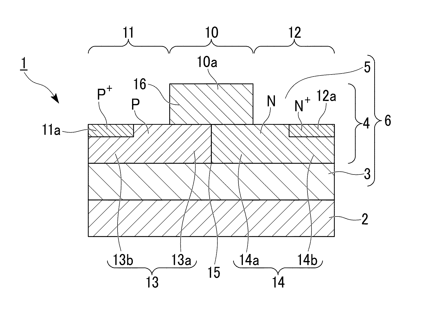
[0118]FIG. 1A is a cross-sectional view showing an optical element according to the first embodiment of the present invention. In addition, FIGS. 2A, 2B, and 3 show a configuration example in which electrodes are provided to the optical element.

[0119]FIG. 1A and FIG. 2A show a cross-sectional view showing a section perpendicular to the advancing direction of light (longitudinal direction of the optical waveguide). In the present embodiment, an SOI (Silicon On Insulator) substrate made of silicon (Si)-silica (SiO2)-silicon (Si) can be used as a substrate for use in manufacturing. A lower cladding 3 of the optical waveguide 6 is formed from SiO2 in the middle of the SOI substrate and the core 4 is formed from the upper Si layer. The lower Si layer forms a substrate 2.

[0120]The core 4 is a rib silicon waveguide and includes the rib part 10 which is thick at the center. Light transmitted into the waveguide will be distributed centering on the rib part 10.

[0121]On the other hand, the sla...

second embodiment

[0138]By calculating Δn / Δα based on the above-described Equation 1 and Equation 2 with neglecting the change in electron density ΔNe, it is found that Δn / Δα is approximately inversely proportional to the hole density ΔNh to the power of 0.2 [i.e., Δn / Δα∝1 / (ΔNh)0.2] in the P-type region. On the other hand, in the N-type region, with neglecting the change in hole density ΔNh, Δn / Δα stays approximately constant regardless of the electron density ΔNe.

[0139]These relationships are shown in a graph in FIG. 17. It is noted that the horizontal axis in FIG. 17 represents the carrier density, in which ΔNe is used for electrons and ΔNh is used for holes. In addition, the numbers in FIG. 17 are expressed in a manner that 1×10±m is 1E±m (±m is an integer).

[0140]As is clear from FIG. 17, since Δn / Δα is high in the P-type low-concentration region, it is possible to increase Δn / Δα and reduce the amount of the change in loss by increasing the proportion of the P-type low-concentration doping region ...

third embodiment

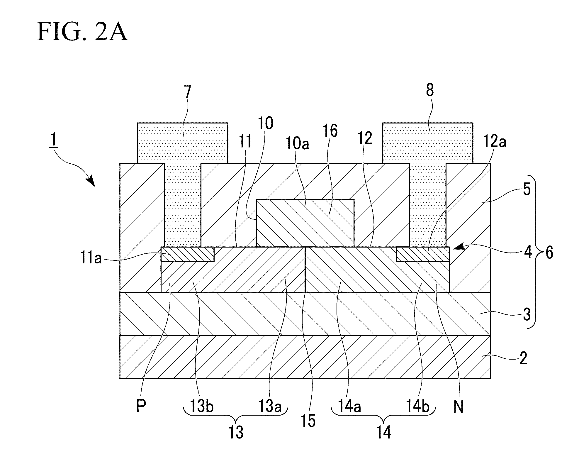
[0144]In the first and second embodiments, the high-concentration doping region for making contact with the metal electrodes 7 and 8 is formed in the upper part of the slab parts 11 and 12. Since absorption of light in the metal material used for the electrodes 7 and 8 is large, it is required to separate the electrodes 7 and 8 sufficiently from the region in which guided light will be distributed, in order to reduce the absorption. However, as separating the electrodes 7 and 8 from the region in which guided light will be distributed, the distance between the electrodes 7 and 8 and the PN junction part 15 becomes larger. This will increase the resistance value in the semiconductor between the electrodes 7 and 8 and the PN junction part 15 and cause reduction of the response speed of the semiconductor constituting the core, or the like, resulting in deterioration of the high frequency characteristic.

[0145]In view of the above, as shown in FIG. 6, it may be possible to arrange contac...


PUM

PropertyMeasurementUnit
refractive indexaaaaaaaaaa
concentrationaaaaaaaaaa
heightaaaaaaaaaa

Abstract

Provided is an optical element including an optical waveguide including a core formed from: a rib part; and a first and second slab parts sandwiching the rib part. The first slab part includes a P-type region, the second slab part includes an N-type region, the rib part includes a P-type region which is in contact with the P-type region provided in the first slab part, and an N-type region which is in contact with the N-type region provided in the second slab part. The rib part includes a top portion which is located above the first and second slab parts and includes an undoped region formed from at least one of an intrinsic region and a low-concentration doping region which is doped at a dopant concentration 1/10 or less of a dopant concentration in at least one of the adjacent P-type region and the adjacent N-type region.

Description

CROSS REFERENCE TO RELATED APPLICATIONS[0001]This application is a continuation application based on a PCT Patent Application No. PCT / JP2012 / 077761, filed Oct. 26, 2012, whose priority is claimed on Japanese Patent Application No. 2011-234964, filed Oct. 26, 2011, the entire content of which are hereby incorporated by reference.BACKGROUND OF THE INVENTION[0002]1. Field of the Invention[0003]The present invention relates to an optical element and a Mach-Zehnder optical waveguide element using the same for use, for example, in optical communications.[0004]2. Description of the Related Art[0005]Recently, the amount of information in optical communications has been increasing. In order to cope with the increase in the amount of information, measures such as the improvement of the signal speed and increase of the number of channels using wavelength multiplex communication have been taken in various type of optical communication networks such as backbone network, metro network, and access...

Claims


Application Information

Patent Timeline
Patent Type & Authority Applications(United States)
IPC IPC(8): G02F1/225G02B6/122
CPCG02F1/2257G02F2001/212G02B2006/12061G02B6/122G02B6/2935G02B2006/12159G02F1/025G02F2201/063G02F1/0151G02F1/212G02B2006/12097G02B2006/12142
Inventor GOI, KAZUHIROOGAWA, KENSUKE
Owner THE FUJIKURA CABLE WORKS LTD
Why Eureka
Try Eureka