Method and control chip for performing access control of memory device

a control chip and memory device technology, applied in the direction of unauthorized memory use protection, instruments, computing, etc., can solve the problem of removing the advantages of using the pcie interface, and achieve the effect of preventing information security related attacks

Active Publication Date: 2021-03-04
REALTEK SEMICON CORP
View PDF0 Cites 2 Cited by
  • Summary
  • Abstract
  • Description
  • Claims
  • Application Information

AI Technical Summary

Benefits of technology

[0004]An objective of the present invention is to provide a method and a control chip for performing access control of a memory device, to solve the problem of the trade-off between information security and performance; in particular, the advantages of a Peripheral Component Interconnect Express (PCIe) interface, such as transmission speed.
[0008]The present invention can establish a protection mechanism regarding DMA attacks with the aid of permissions management and / or a determination mechanism within an initialization procedure, which enables an electronic device (e.g. a personal computer) equipped with the PCIe interface to have the specific ability of preventing information security related attacks when a user (more particularly, a user having general information security concept) operates this electronic device. Thus, the present invention can solve the problem of the related art without introducing any side effect or in a way that is less likely to introduce side effects.

Problems solved by technology

Although this protects the user from unwanted DMA attacks, this also removes the advantages of using the PCIe interface.

Method used


Image

  • Method and control chip for performing access control of memory device
  • Method and control chip for performing access control of memory device
  • Method and control chip for performing access control of memory device

Examples


Embodiment Construction

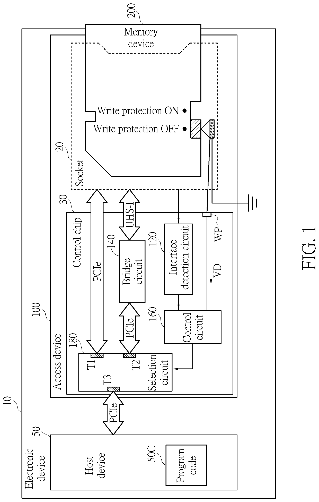
[0015]FIG. 1 is a diagram illustrating a memory device 200 being inserted into an electronic device 10 according to an embodiment of the present invention. In this embodiment, examples of the electronic device 10 may include, but are not limited to: a laptop computer, a tablet or a mobile phone, and the memory device 200 may be a memory card conforming to a secure digital (SD) specification, but the present invention is not limited thereto. The electronic device 10 comprises a host device 50 and an access device 100 (e.g. a card reader) coupled to the host device 50, where the host device 50 may control operations of the access device 100 according to a program code 50C (e.g. a program module of an operating system (OS) of the electronic device 10 and / or a driver program corresponding to the access device 100). In addition, the access device 100 may comprise a socket 20 and a control chip 30 coupled to the socket 20, where the socket 20 may be configured to connect the control chip ...


PUM


Abstract

A method and a control chip for performing access control of a memory device are provided, wherein the control chip is coupled to a host device. The method includes: utilizing a first transmission interface of the control chip to determine whether the memory device supports a second transmission interface different from the first transmission interface to generate a determination result; and according to user permissions of a user regarding the host device, determining whether to allow the control chip to decide whether to utilize the second transmission interface to access the memory device based on the determination result. In addition, if the user permissions satisfy a predetermined condition, a user interface of the host device may display a pop-up window in order to allow the user to decide which one of the first transmission interface and the second transmission interface to utilize for accessing the memory device.

Description

BACKGROUND OF THE INVENTION1. Field of the Invention[0001]The present invention is related to access control of memory devices, and more particularly, to a method and a control chip for performing access control of a memory device.2. Description of the Prior Art[0002]Peripheral Component Interconnect Express (PCIe) interfaces are general high speed interfaces used in electronic devices, which are reliable due to decades of development. A PCIe interface may be configured for communication between a system and peripheral devices. As it is scalable, the PCIe interface can also be applied to ports outside a case (e.g. a computer case), allowing some removable devices (e.g. external devices) to be connected with the system via the PCIe interface, so that the user can enjoy the benefit of the PCIe interface without needing to open the case. For example, an interface conforming to the ExpressCard specification configures the PCIe interface to be used by external devices.[0003]Utilizing an ...

Claims


Application Information

Patent Timeline
Patent Type & Authority Applications(United States)
IPC IPC(8): G06F12/14G06F12/1081G06F21/79G06F9/451G06F13/16G06F13/40G06F13/42
CPCG06F12/1458G06F12/1081G06F21/79G06F2221/2113G06F13/1694G06F13/4022G06F13/4221G06F9/451G06F2212/1052G06F12/1483G06F12/1491G06F12/0246G06F2212/7208G06F12/1433
Inventor SHIAU, JIUNN-HUNGLIN, NENG-HSIENCHEN, CHENG-CHANG
Owner REALTEK SEMICON CORP
Why Eureka
Try Eureka