

Laser irradiation apparatus and laser irradiation method
a laser irradiation and laser technology, applied in laser beam welding apparatus, solid-state devices, manufacturing tools, etc., can solve problems such as restricted layou
- Summary
- Abstract
- Description
- Claims
- Application Information
AI Technical Summary
Benefits of technology
Problems solved by technology
Method used
Image

Examples
embodiment mode 1
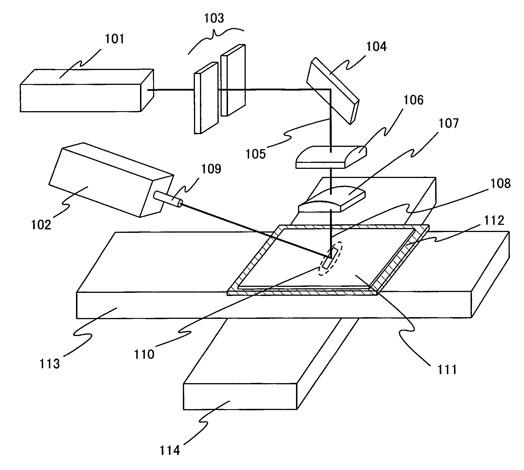
[0055]This embodiment mode is described with reference to FIG. 1 and FIGS. 3A to 3F. According to the present invention, when laser annealing is conducted to a semiconductor film with a CW linear laser beam of a harmonic, opposite end portions of the CW linear beam are blocked by a slit. At the same time, a CW laser beam of the fundamental wave is delivered so that the laser beams of the harmonic and the fundamental wave overlap with each other on an irradiation surface.
[0056]Laser oscillators 101 and 102 are known CW laser oscillators. For example, a laser whose medium is a single-crystal YAG, YVO4, YLF, YAlO3, or GdVO4, or a poly-crystal YAG, Y2O3, YVO4, YAlO3, or GdVO4, each of which is added with one or plural elements selected from the group consisting of Nd, Yb, Cr, Ti, Ho, Er, Tm, and Ta as dopant can be used. Moreover, another solid-state laser such as an alexandrite laser or a Ti: sapphire laser or a semiconductor laser such as a GaN laser, a GaAs laser, or an IsAs laser ca...
embodiment 1
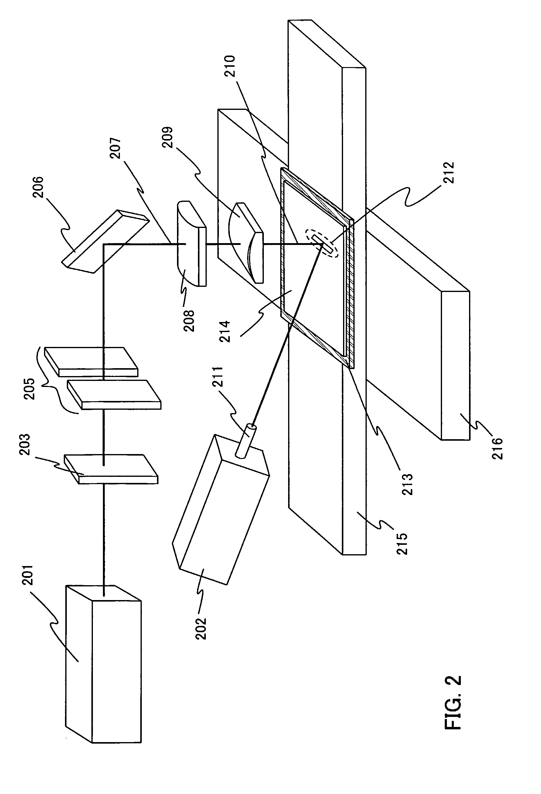
[0070]In this embodiment, a diffractive optical element (also referred to as diffractive optics or a diffractive optics element) is used to crystallize a semiconductor film more homogeneously. A harmonic of a CW laser beam is shaped into a linear or rectangular laser beam having homogeneous energy distribution with the use of the diffractive optical element, opposite end portions of this laser beam are blocked by a slit, and then the laser beam is delivered to a semiconductor film. In addition, a CW laser beam of the fundamental wave is delivered simultaneously so as to overlap the linear or rectangular beam on an irradiation surface.
[0071]A laser irradiation apparatus shown in this embodiment comprises laser oscillators 201 and 202, a diffractive optical element 203, a slit 205, a mirror 206, condensing lenses 208 and 209, a suction stage 213, an X-stage 215, and a Y-stage 216.
[0072]FIG. 2 shows an example of the laser irradiation apparatus. First, a substrate 214 over which an amo...
embodiment 2
[0091]In this embodiment, laser beams emitted from two CW laser oscillators of a harmonic are divided and the laser beams with different energy distribution are overlapped with each other so that a laser beam having homogeneous energy distribution is formed. Moreover, after further homogenizing the energy distribution of the laser beam by blocking end portions of the laser beam with the use of a slit, the laser beam is delivered to a semiconductor film. At the same time, a CW laser beam of the fundamental wave is delivered so as to overlap the laser beam of the harmonic on an irradiation surface. This summary is described with reference to FIG. 5 and FIGS. 6A to 6C.
[0092]Reference numerals 501 and 502 denote laser oscillators. The laser oscillators 501 and 502 are known CW laser oscillators such as a laser having a medium of a single-crystal YAG, YVO4, YLF, YAlO3, or GdVO4, or a poly-crystal YAG, Y2O3, YVO4, YAlO3, or GdVO4, each of which is added with one or plural elements selecte...
PUM
| Property | Measurement | Unit |
|---|---|---|
| aspect ratio | aaaaa | aaaaa |
| aspect ratio | aaaaa | aaaaa |
| thickness | aaaaa | aaaaa |
Abstract
Description
Claims
Application Information