Electron emission display device and control method of the same

a technology of display device and electron emission, which is applied in the direction of instruments, static indicating devices, etc., can solve the problems of insufficient brightness control or maintenan

Inactive Publication Date: 2010-10-12
SAMSUNG SDI CO LTD
View PDF11 Cites 2 Cited by
  • Summary
  • Abstract
  • Description
  • Claims
  • Application Information

AI Technical Summary

Benefits of technology

[0018]Accordingly, an aspect of the present invention provides an electron emission display device capable of providing more even (or uniform or exact) compensation of the pixels, and a control method of the same.

Problems solved by technology

Also, the brightness may still not be properly controlled (or maintained) because no input data signal is added to the pixel 5 displaying the brightness of ‘10’.

Method used


Image

  • Electron emission display device and control method of the same
  • Electron emission display device and control method of the same
  • Electron emission display device and control method of the same

Examples


Embodiment Construction

[0035]In the following detailed description, certain exemplary embodiments of the present invention are shown and described, by way of illustration. As those skilled in the art would recognize, the described exemplary embodiments may be modified in various ways, all without departing from the spirit or scope of the present invention. Accordingly, the drawings and description are to be regarded as illustrative in nature, rather than restrictive.

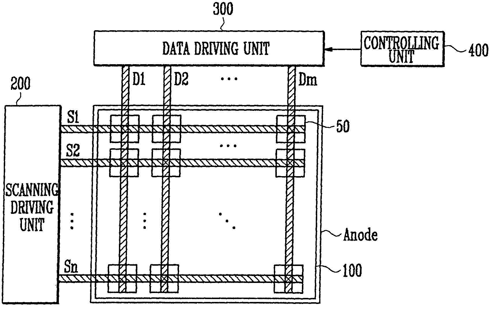
[0036]FIG. 4 is a diagram showing one embodiment of an electron emission display device according to the present invention.

[0037]Referring to FIG. 4, the electron emission display device according to the present invention includes a display region 100, a scanning driving unit 200, a data driving unit 300, and a controlling unit 400.

[0038]The display region 100 includes a plurality of scanning lines (S1, S2, . . . Sn), a plurality of data lines (D1, D2, . . . Dm), and an anode. In addition, a plurality of pixels 50 are formed in regions defined...


PUM


Abstract

An electron emission display device and a control method of the same. The electron emission display device includes a display region having a plurality of scanning lines and a plurality of data lines; a plurality of pixels arranged in regions defined by the scanning lines and the data lines; a data driving unit for transmitting a data signal to the data lines; a scanning driving unit for transmitting a scanning signal to the scanning lines; and a controlling unit for identifying display data for indicating a brightness displayed by the pixels, and correcting the input data input into the pixels using compensation coefficients corresponding to the pixels. In this electron emission device, the input data is corrected in the controlling unit by multiplying the compensation coefficients by the input data.

Description

CROSS-REFERENCE TO RELATED APPLICATION[0001]This application claims priority to and the benefit of Korean Patent Application No. 10-2005-0072506, filed on Aug. 8, 2005, in the Korean Intellectual Property Office, the entire content of which is incorporated herein by reference.BACKGROUND[0002]1. Field of the Invention[0003]The present invention relates to an electron emission display device and a control method of the same, and in particular, to an electron emission display device for controlling brightness characteristics in pixels so as to improve uneven light emission between the pixels, and a control method of the same.[0004]2. Discussion of Related Art[0005]An electron emission display device is a flat panel display device that is composed of a cathode, an anode and a gate electrode. More particularly, the cathode usually used as a scanning electrode is formed on a substrate. An insulating layer including an aperture (or a hole) and the gate electrode usually used as a data elec...

Claims


Application Information

Patent Timeline
Patent Type & Authority Patents(United States)
IPC IPC(8): G09G3/20
CPCG09G3/22G09G2320/0233G09G2320/0271G09G2320/0285G09G2320/029G09G3/20
Inventor LEE, JI WON
Owner SAMSUNG SDI CO LTD
Why Eureka
Try Eureka