

Light emitting diode package structure
a technology of light-emitting diodes and package structures, applied in the field of package structures, can solve the problems of reducing the inability of conventional phosphor powder coating methods to meet the current requirements, and the inability to achieve the consistency of spatial spectral distribution and illumination brightness, etc., to achieve the effect of improving the overall luminance performance of led package devices, improving the reliability of led package structures, and improving the uniformity of reflected ligh
- Summary
- Abstract
- Description
- Claims
- Application Information
AI Technical Summary
Benefits of technology
Problems solved by technology
Method used
Image

Examples
first embodiment
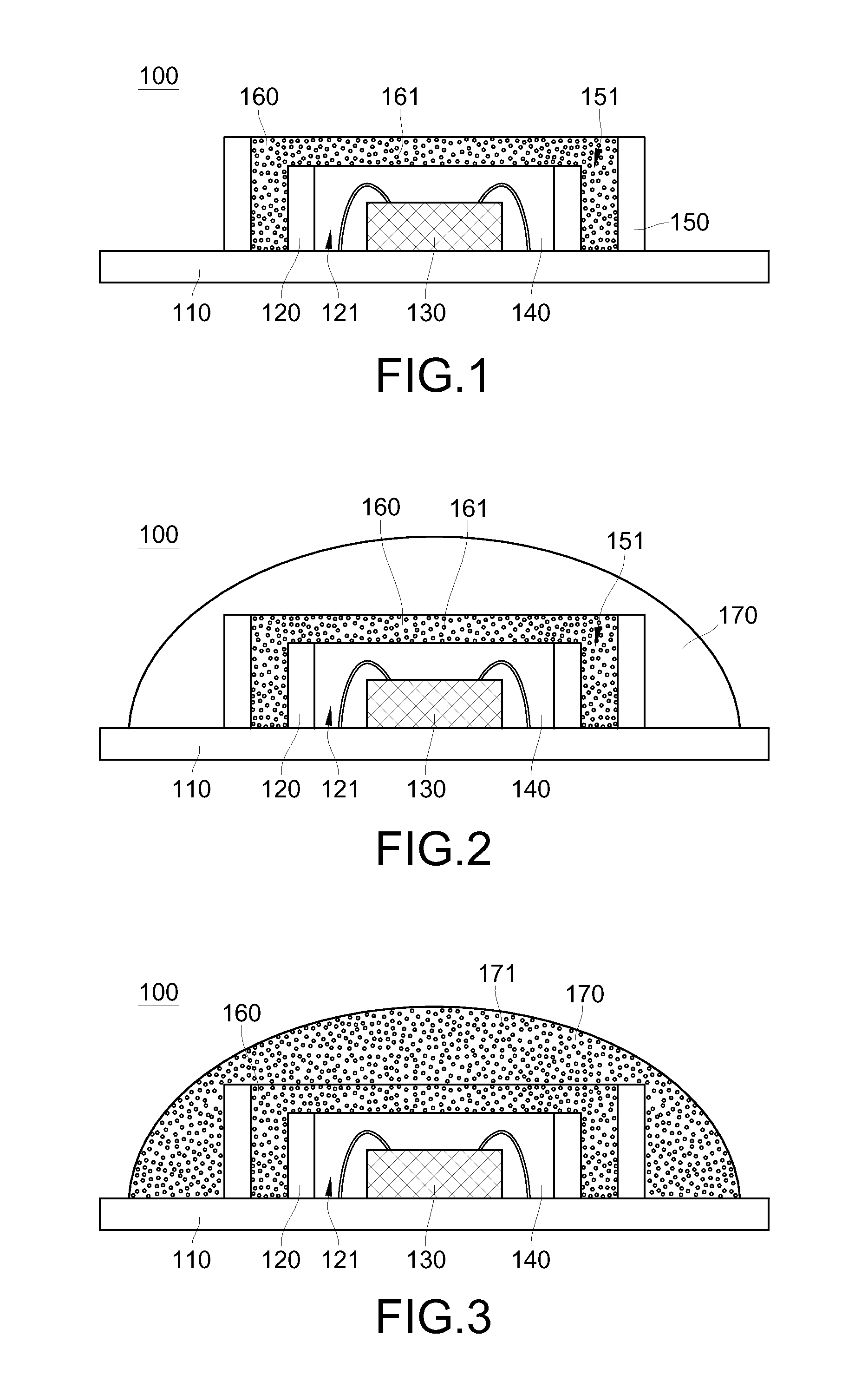
[0039]FIGS. 2 and 3 are side cross-sectional views of different aspects according to the present invention, and the implementation aspects disclosed in FIGS. 2 and 3 substantially have the same structure as the embodiment in FIG. 1, and only the differences between FIGS. 1, 2 and 3 would be described below.
[0040]As shown in FIG. 2, in addition to the substrate 110, the first enclosure 120, the LED 130, the first package material 140, the second enclosure 150, and the second package material 160, the LED package structure 100 of the present embodiment further includes a lens 170. The lens 170 covers the second enclosure 150 and the second package material 160, and the material of the lens 170 is a transparent material, for example, but not limited to, a polymer material or a glass material. The illuminating light emitted by the LED 130 is reflected to a wall surface of the lens 170, so the lens 170 can provide a better use of reflecting light.
[0041]Furthermore, as shown in FIG. 3, th...
second embodiment
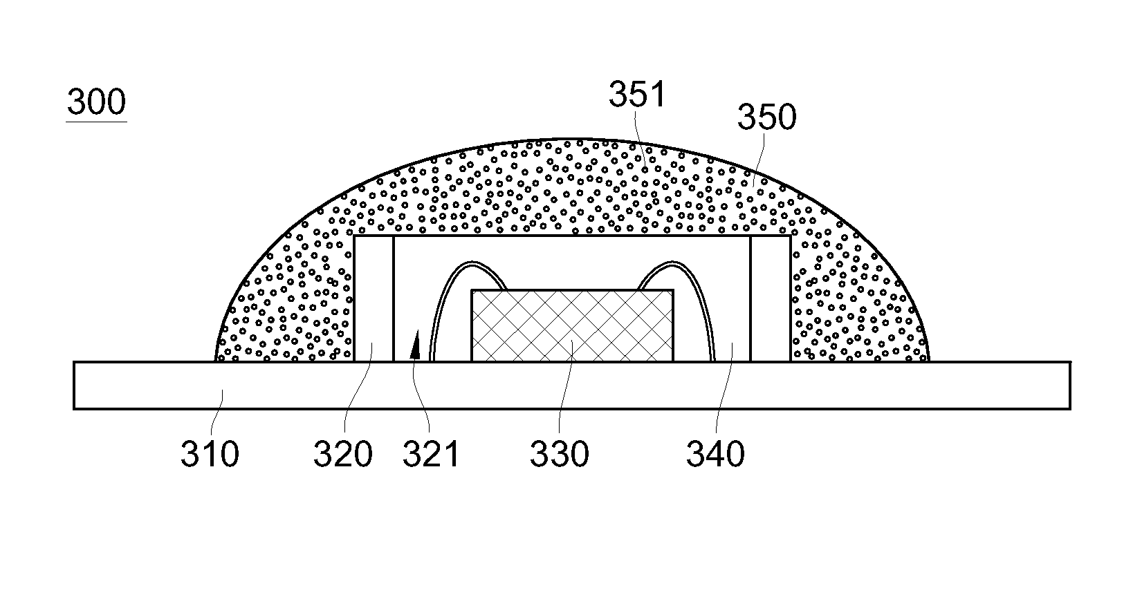
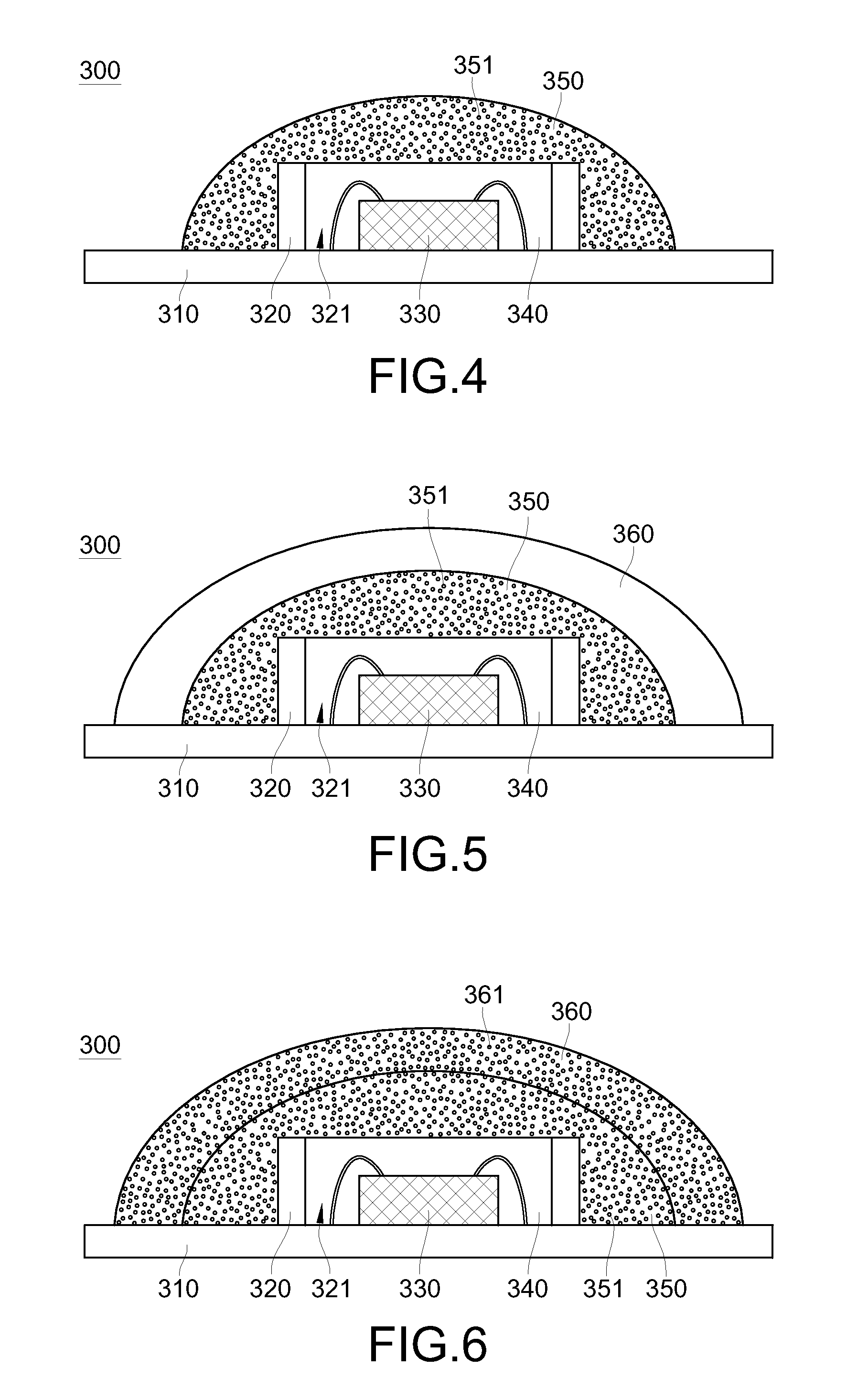
[0050]FIGS. 5 and 6 are side cross-sectional views of different aspects according to the present invention, and the implementation aspects disclosed in FIGS. 5 and 6 have substantially the same structure as the embodiment in FIG. 4, and only the differences between FIGS. 5 and 6 would be described illustrated below.
[0051]As shown in FIG. 5, in addition to the substrate 310, the enclosure 320, the LED 330, the first package material 340, and the second package material 350, the LED package structure 300 further includes a lens 360. The lens 360 covers the second package material 350, and the material of the lens 360 is transparent material, for example, but not limited to, a polymer material and a glass material. The illuminating light emitted by the LED 330 is reflected on a wall surface of the lens 360, so the lens 360 provides a better use of reflected light.
[0052]Furthermore, as shown in FIG. 6, the lens 360 of the present embodiment may further have a second fluorescent material...
PUM
 Abstract
Description
Claims
Application Information