Light-emitting device and method for manufacturing light-emitting device
a technology of light-emitting devices and manufacturing methods, which is applied in the direction of sustainable manufacturing/processing, climate sustainability, semiconductor devices, etc., can solve problems such as erode reliability, and achieve the effect of high reliability
- Summary
- Abstract
- Description
- Claims
- Application Information
AI Technical Summary
Benefits of technology
Problems solved by technology
Method used
Image

Examples
embodiment 1
[0053]In this embodiment, a flexible light-emitting device of one embodiment of the present invention and a method for manufacturing the light-emitting device will be described with reference to FIGS. 1A to 1C, FIGS. 2A to 2C, FIGS. 3A1, 3A2, 3B, and 3C, FIGS. 4A and 4B, FIGS. 5A and 5B, FIGS. 6A to 6D, FIGS. 7A to 7D, FIGS. 8A to 8D, FIGS. 9A to 9D, FIGS. 10A to 10D, FIGS. 11A, 11B1, 11B2, 11B3, 11B4, and 11C, and FIGS. 12A to 12F.
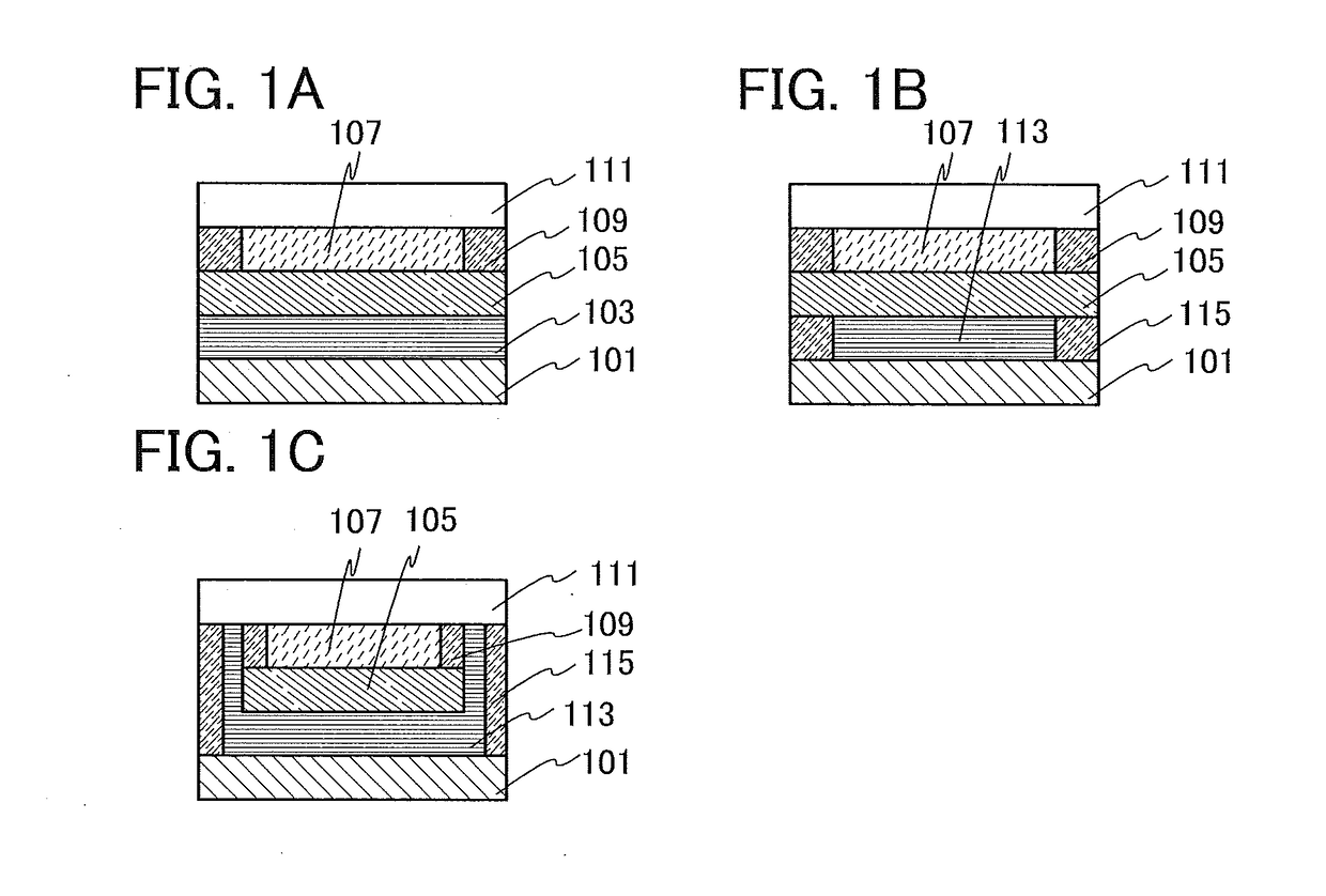
[0054]The light-emitting device of one embodiment of the present invention includes a light-emitting element sealed by a pair of flexible substrates and a bonding layer.
[0055]The bonding layer is not covered at a side surface of the light-emitting device. For this reason, impurities such as moisture and oxygen enter an organic EL element from the outside when the bonding layer has a low gas barrier property. The entry of impurities into the organic EL element causes, for example, shrinkage of a light-emitting portion (here, luminance degradation from an e...
example 1
Structural Example 1
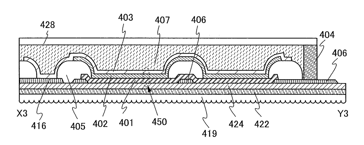
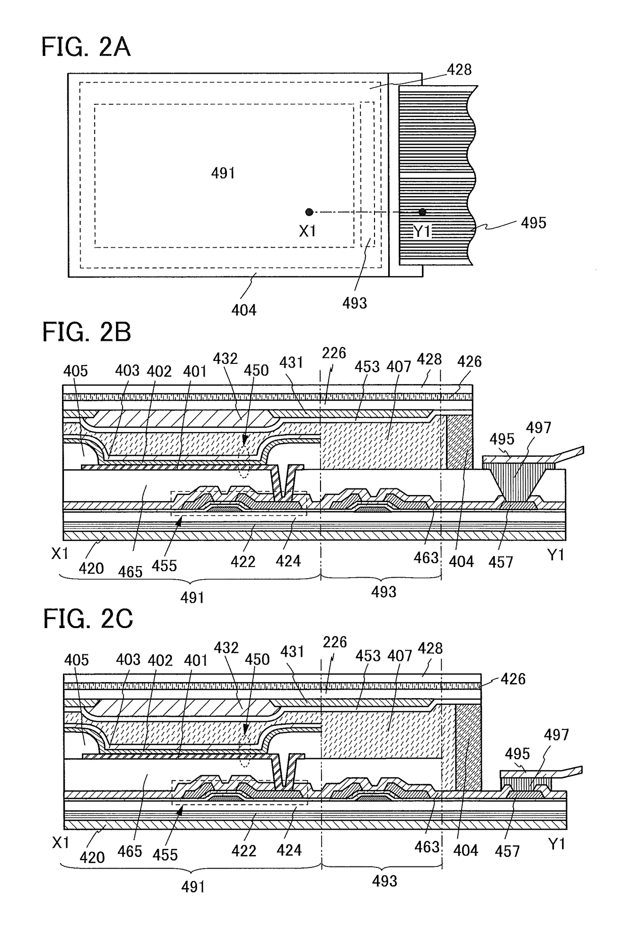
[0069]FIG. 2A is a plan view of a light-emitting device. FIGS. 2B and 2C are each an example of a cross-sectional view taken along dashed-dotted line X1-Y1 in FIG. 2A. The light-emitting devices illustrated in FIGS. 2A to 2C are top-emission light-emitting devices using a color filter method.
[0070]The light-emitting device illustrated in FIG. 2A includes a light-emitting portion 491, a driver circuit portion 493, and a flexible printed circuit (FPC) 495. An organic EL element and a transistor included in the light-emitting portion 491 and the driver circuit portion 493 are sealed by a flexible substrate 420, a flexible substrate 428, a first bonding layer 407, and a second bonding layer 404.
[0071]The light-emitting devices illustrated in FIGS. 2B and 2C each include the flexible substrate 420, an adhesive layer 422, an insulating layer 424, a transistor 455, an insulating layer 463, an insulating layer 465, an insulating layer 405, an organic EL element 450 (a fi...
example 2
Structural Example 2
[0081]FIG. 3A1 is a plan view of the light-emitting device, and FIG. 3B is a cross-sectional view taken along dashed-dotted line X21-Y21 in FIG. 3A1. The light-emitting device illustrated in FIG. 3B is a top-emission light-emitting device using a separate coloring method.
[0082]The light-emitting device illustrated in FIG. 3A1 includes the light-emitting portion 491, the driver circuit portion 493, and the FPC 495. An organic EL element and a transistor included in the light-emitting portion 491 and the driver circuit portion 493 are sealed by the flexible substrate 420, the flexible substrate 428, the first bonding layer 407, and the second bonding layer 404. FIG. 3B illustrates an example where the conductive layer 457 and the connector 497 are connected to each other through an opening portion of the second bonding layer 404.
[0083]The light-emitting device illustrated in FIG. 3B includes the flexible substrate 420, the adhesive layer 422, the insulating layer 4...
PUM
 Abstract
Description
Claims
Application Information
 - R&D
- Intellectual Property
- Life Sciences
- Materials
- Tech Scout
- Unparalleled Data Quality
- Higher Quality Content
- 60% Fewer Hallucinations
Browse by: Latest US Patents, China's latest patents, Technical Efficacy Thesaurus, Application Domain, Technology Topic, Popular Technical Reports.
© 2025 PatSnap. All rights reserved.Legal|Privacy policy|Modern Slavery Act Transparency Statement|Sitemap|About US| Contact US: help@patsnap.com