Method of repairing display substrate and display substrate repaired by the method

a display substrate and repair method technology, applied in the direction of electrical equipment, semiconductor devices, instruments, etc., can solve the problems of difficult repair of signal lines, deterioration of display quality of lcd panels, and difficulty in repairing signal lines, so as to achieve exquisite repair of display substrates

Active Publication Date: 2018-04-03
SAMSUNG DISPLAY CO LTD
View PDF10 Cites 0 Cited by
  • Summary
  • Abstract
  • Description
  • Claims
  • Application Information

AI Technical Summary

Benefits of technology

[0014]According to an exemplary embodiment, a method of repairing a display substrate uses an ultra-fast laser to selectively remove an organic layer overlapping the gate metal pattern or the data metal pattern having defects, such that defects of display substrate may be repaired exquisitely.
[0015]According to an exemplary embodiment, a method of repairing a display substrate also includes forming a light-blocking portion in a peripheral area of the repair hole, which may block light leakage through the repair hole.

Problems solved by technology

The signal line of the array substrate may have an electrical connection failure such as a short circuit, a shorting failure, etc., which may deteriorate a display quality of the LCD panel.
Therefore, it may be necessary to repair the signal line having the electrical connection failure.
However, when a color filter is disposed on the same lower substrate as the gate line and the data line, the color filter may cover the data line, which may render repairing the signal line difficult.
In addition, when the repair line is not in contact with the data line, repairing the defects may be almost impossible.

Method used


Image

  • Method of repairing display substrate and display substrate repaired by the method
  • Method of repairing display substrate and display substrate repaired by the method
  • Method of repairing display substrate and display substrate repaired by the method

Examples


Embodiment Construction

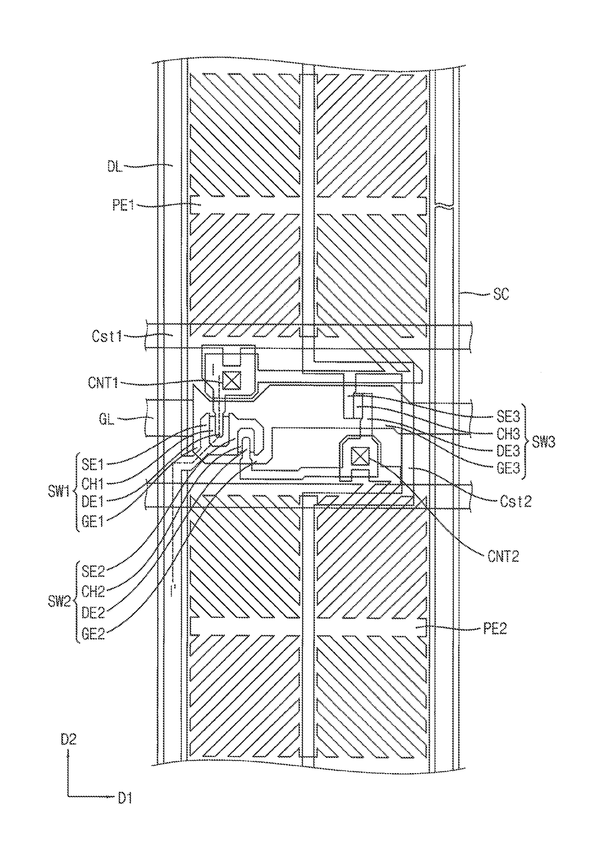
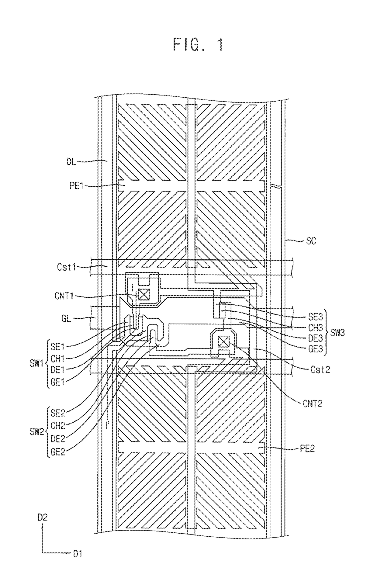
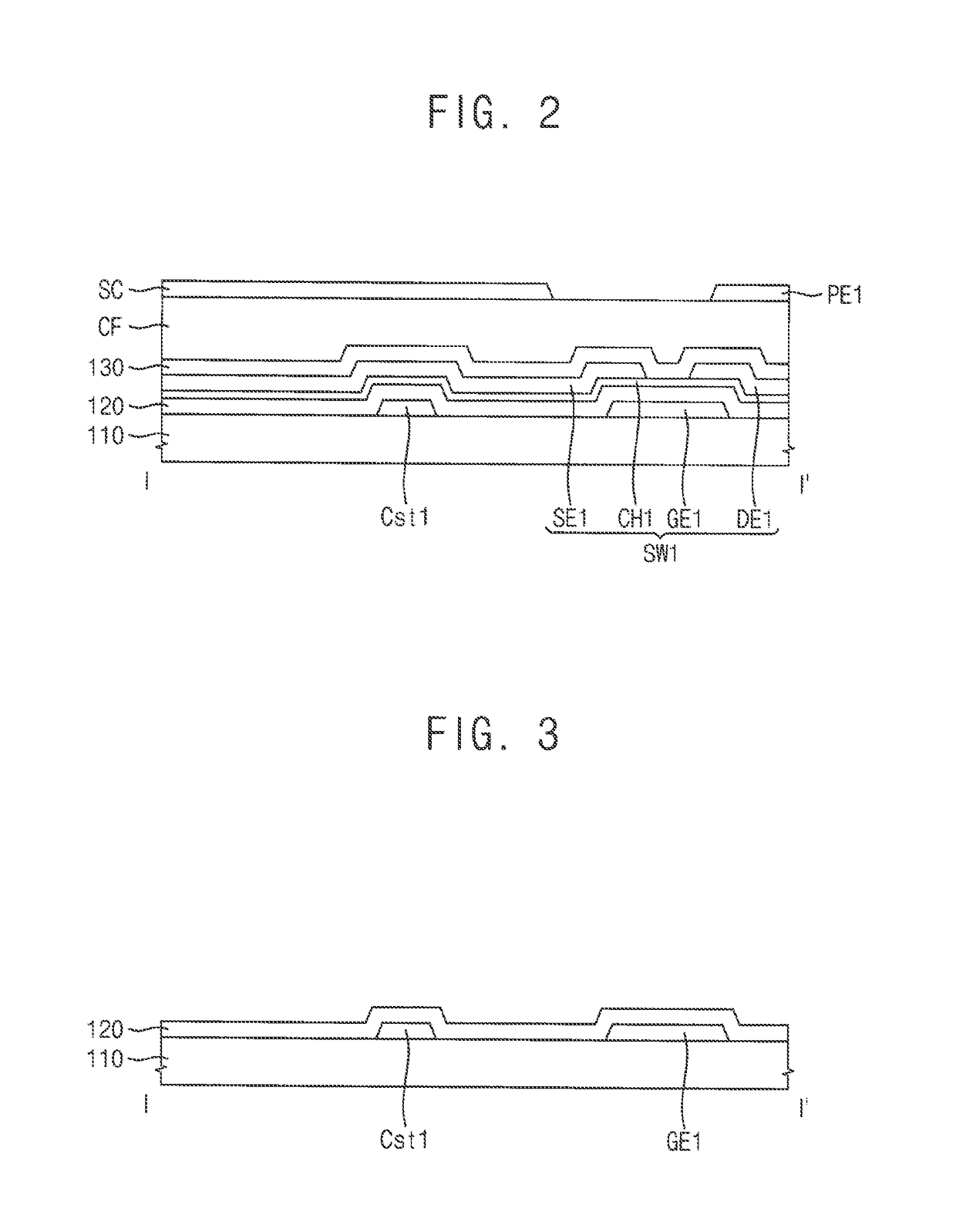
[0049]In the following description, for the purposes of explanation, numerous specific details are set forth in order to provide a thorough understanding of various exemplary embodiments. It is apparent, however, that various exemplary embodiments may be practiced without these specific details or with one or more equivalent arrangements. In other instances, well-known structures and devices are shown in block diagram form in order to avoid unnecessarily obscuring various exemplary embodiments.

[0050]In the accompanying figures, the size and relative sizes of layers, films, panels, regions, etc., may be exaggerated for clarity and descriptive purposes. Also, like reference numerals denote like elements.

[0051]When an element or layer is referred to as being “on,”“connected to,” or “coupled to” another element or layer, it may be directly on, connected to, or coupled to the other element or layer or intervening elements or layers may be present. When, however, an element or layer is re...


PUM

PropertyMeasurementUnit
areasaaaaaaaaaa
areaaaaaaaaaaa
electrical connectionaaaaaaaaaa

Abstract

A display substrate includes a gate metal pattern including a gate line extending in a first direction, a gate electrode electrically connected to the gate line and a storage line, a data metal pattern including a data line extending in a second direction crossing the first direction, a source electrode electrically connected to the data line and a drain electrode spaced apart from the source electrode, an organic layer disposed on the data metal pattern, and a repair hole formed through the organic layer and exposing a portion of the gate metal pattern or a portion of the data metal pattern.

Description

CROSS-REFERENCE TO RELATED APPLICATION[0001]This application claims priority from and the benefit of Korean Patent Application No. 10-2015-0066596, filed on May 13, 2015, which is hereby incorporated by reference for all purposes as if fully set forth herein.BACKGROUND[0002]Field[0003]Exemplary embodiments relate to a method of repairing a display substrate and a display substrate repaired by the method. More particularly, exemplary embodiments relate to a method of repairing a display substrate using an ultra-fast laser and a display substrate repaired by the method.[0004]Discussion of the Background[0005]A liquid crystal display (LCD) panel may generally include a thin-film transistor (TFT) substrate, an opposing substrate, and a liquid crystal (LC) layer. The TFT substrate includes gate lines, data lines crossing the gate lines, TFTs connected with the gate lines and the data lines, and pixel electrodes connected with the TFTs. The TFT may include a gate electrode extended from t...

Claims


Application Information

Patent Timeline
Patent Type & Authority Patents(United States)
IPC IPC(8): H01L27/12G02F1/1343G02F1/1368G02F1/1335G02F1/1333H01L29/786G02F1/1362
CPCG02F1/136259G02F1/1368G02F1/13439G02F1/133345G02F1/133514G02F1/134309G02F1/136286H01L27/1244H01L27/1248H01L27/1259H01L29/78633G02F1/136227G02F2001/136263G02F2001/136218H01L27/1225H01L27/1255G02F1/136263G02F1/136218
Inventor SONG, IN-CHEOLHAN, JAE-MINLEE, HYUNG-SUK
Owner SAMSUNG DISPLAY CO LTD
Why Eureka
Try Eureka