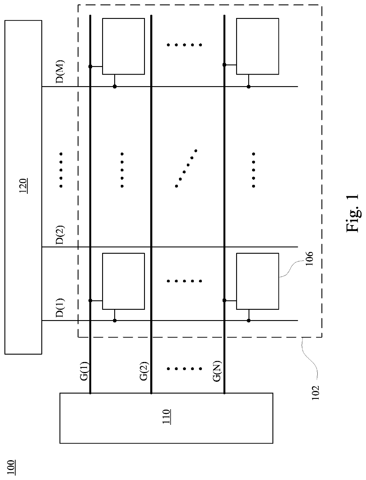
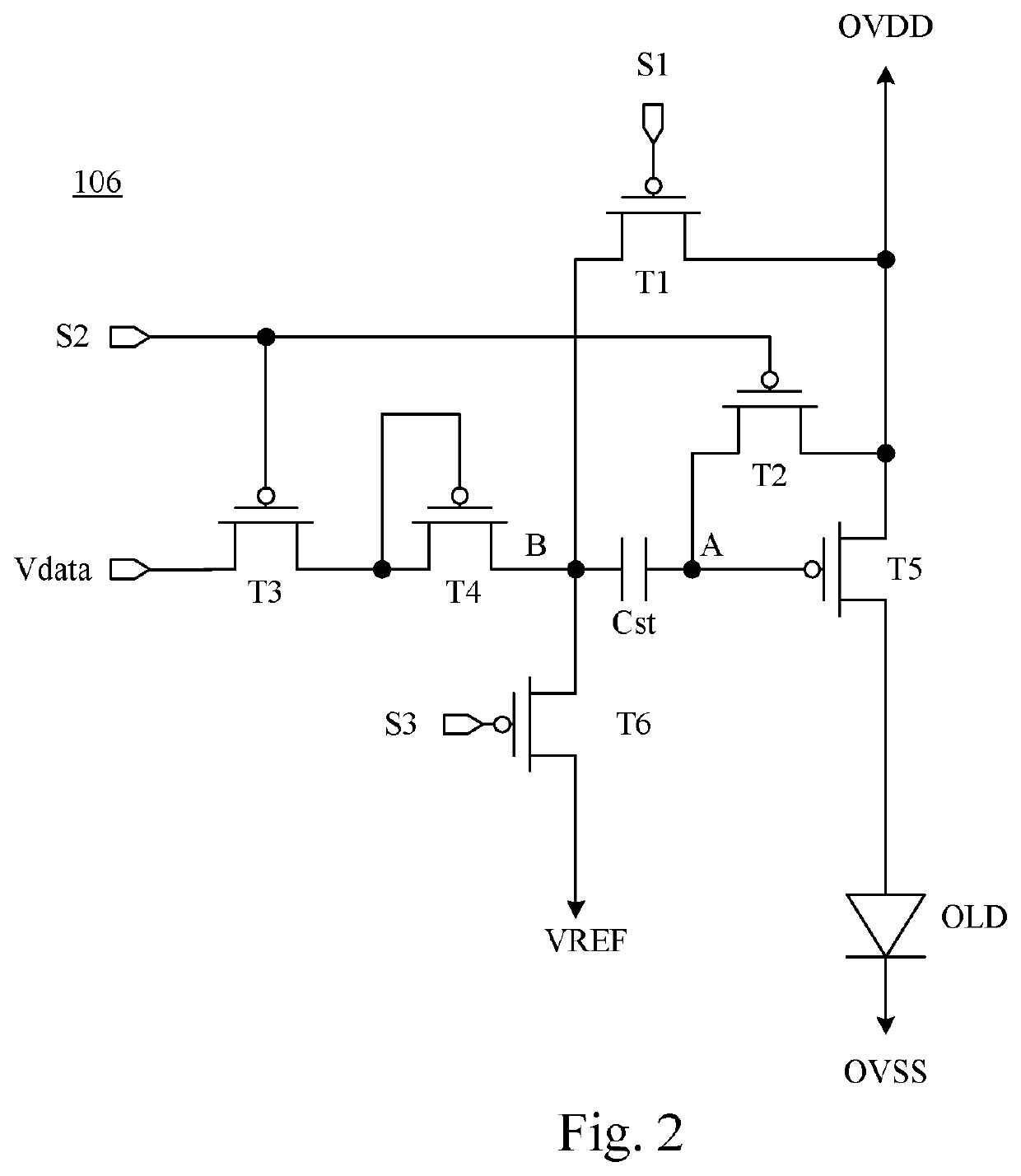
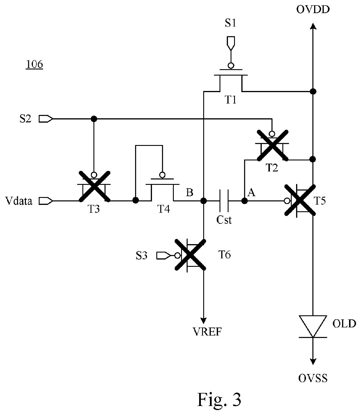
Pixel circuit

a pixel circuit and pixel technology, applied in the field of pixel circuits, can solve problems such as unfavorable display devices and mura defects, and achieve the effect of avoiding mura defects of display devices and avoiding threshold voltage offset of driving transistors

Active Publication Date: 2020-03-31
AU OPTRONICS CORP
View PDF11 Cites 0 Cited by
  • Summary
  • Abstract
  • Description
  • Claims
  • Application Information

AI Technical Summary

Benefits of technology

[0009]Through application of one embodiment described above, a pixel circuit can be realized. By using such a pixel circuit in a display device, mura defects of the display device caused by the threshold voltage offset of the driving transistors can be avoided.

Problems solved by technology

However, threshold voltage offsets of the driving transistors in different pixel driving circuits may exist due to manufacturing processes.
These offsets may cause uneven brightness of the organic light emitting diodes, and ultimately result in mura defects.

Method used


Image

  • Pixel circuit
  • Pixel circuit
  • Pixel circuit

Examples


Embodiment Construction

[0024]Reference will now be made in detail to the present embodiments of the invention, examples of which are illustrated in the accompanying drawings. Wherever possible, the same reference numbers are used in the drawings and the description to refer to the same or like parts.

[0025]It will be understood that, in the description herein and throughout the claims that follow, although the terms “first,”“second,” etc. may be used to describe various elements, these elements should not be limited by these terms. These terms are only used to distinguish one element from another. For example, a first element could be termed a second element, and, similarly, a second element could be termed a first element, without departing from the scope of the embodiments.

[0026]It will be understood that, in the description herein and throughout the claims that follow, when an element is referred to as being “electrically connected” or “electrically coupled” to another element, it can be directly connec...


PUM

PropertyMeasurementUnit
supply voltageaaaaaaaaaa
reference voltageaaaaaaaaaa
voltageaaaaaaaaaa

Abstract

A pixel circuit includes a light emitting component, a storage capacitor, a driving transistor, a first switch, a second switch, a third switch, and a fourth switch. A first end of the driving transistor is configured to receive a supply voltage, and a second end of the driving transistor is electrically connected to an anode end of the light emitting component. The first switch is configured to provide a first reference voltage to a second end of the storage capacitor. The second switch is configured to provide the supply voltage to the first end of the storage capacitor. The third switch and the fourth switch are configured to provide an operating voltage corresponding to a data voltage and a threshold voltage of the third switch to the second end of the storage capacitor.

Description

RELATED APPLICATIONS[0001]This application claims priority to Taiwan Application Serial Number 106141430, filed Nov. 28, 2017, which is herein incorporated by reference.BACKGROUNDTechnical Field[0002]The present disclosure relates to an electronic circuit. More particularly, the present disclosure relates to a pixel circuit.Description of Related Art[0003]With advances in technology, display devices are being increasingly used in our daily lives, such as used in smartphones and computers.[0004]A typical display device may include a gate driving circuit, a source driving circuit, and a pixel circuit array. The gate driving circuit can sequentially provide a plurality of gate signals to the pixel circuits to turn on the switching transistors of the pixel circuits row by row. The source driving circuit can provide a plurality of data signals to the pixel circuits with the switching transistors thereof turned on to enable the pixel circuit to display according to the data signals.[0005]...

Claims


Application Information

Patent Timeline
Patent Type & Authority Patents(United States)
IPC IPC(8): G09G3/3258G09G3/3233
CPCG09G3/3233G09G3/3258G09G2300/0819G09G2320/045G09G2320/0233G09G2310/0251G09G3/3291
Inventor CHENG, MAO-HSUN
Owner AU OPTRONICS CORP
Why Eureka
Try Eureka