

A multilayer ingan quantum dot structure containing a strain-modulated structure
A technology of quantum dots and quantum dot layers, applied in semiconductor devices, electrical components, circuits, etc., can solve the problems of complex strain environment of InGaN quantum dots, poor controllability of quantum dot growth, LED carrier leakage, etc., to achieve Effects of eliminating strain coupling, reducing internal strain, and eliminating strain accumulation
Patent Information
- Authority / Receiving Office
- CN · China
- Patent Type
- Patents(China)
- Current Assignee / Owner
- Publication Date
- 2020-05-05
Smart Images
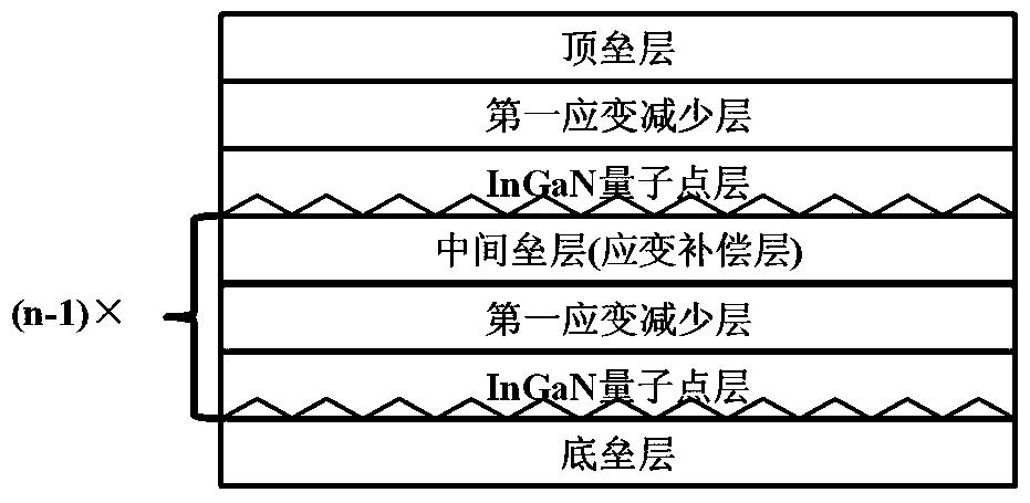
Figure 1 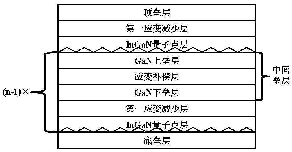
Figure 2 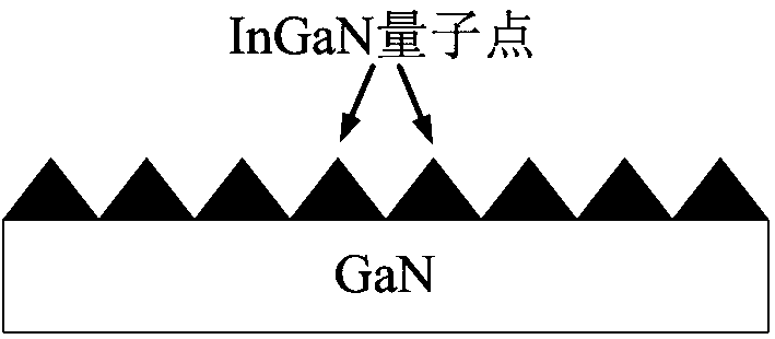
Figure 3
Abstract
Description
technical field
[0001] The invention relates to the field of low-dimensional structures of Group III nitrides, in particular to a multilayer InGaN quantum dot structure containing a strain modulation structure. Background technique
[0002] GaN-based group III nitride materials (including AlN, AlGaN, InN, InGaN, AlGaInN) are the third generation of semiconductor materials after the first generation of silicon germanium, the second generation of gallium arsenide, and indium phosphide. The first-generation semiconductors Si and Ge are the industrial basis of modern microelectronics and integrated circuits; the second-generation GaAs and InP are the basis of red, infrared, mid-infrared and terahertz optoelectronic devices (including lasers, LEDs, detectors, etc.) Material. Group III nitrides (III-N) cover the violet, blue, green, yellow and ultraviolet bands of visible light. Among them, blue light and green light, as the three primary colors, have attracted the attention of ...
Examples
Embodiment Construction
[0027] In order to make the purpose, technical solutions and advantages of the embodiments of the present invention clearer, the technical solutions in the embodiments of the present invention will be clearly and completely described below. Obviously, the described embodiments are part of the embodiments of the present invention, rather than All the embodiments; based on the embodiments of the present invention, all other embodiments obtained by persons of ordinary skill in the art without creative work all belong to the protection scope of the present invention.
[0028] Aiming at the complex strain environment and low density of states of InGaN quantum dots, the present invention introduces a strain modulation structure (including a strain reduction structure and a strain compensation structure) into a multilayer InGaN quantum dot, and provides a multi-layered InGaN quantum dot with a strain modulation structure. The layered InGaN quantum dot structure provides a new type of ...