
Semiconductor device
Patent Information
- Authority / Receiving Office
- US · United States
- Current Assignee / Owner
- Publication Date
- 2007-10-04
- Estimated Expiration
- Not applicable · inactive patent
Smart Images
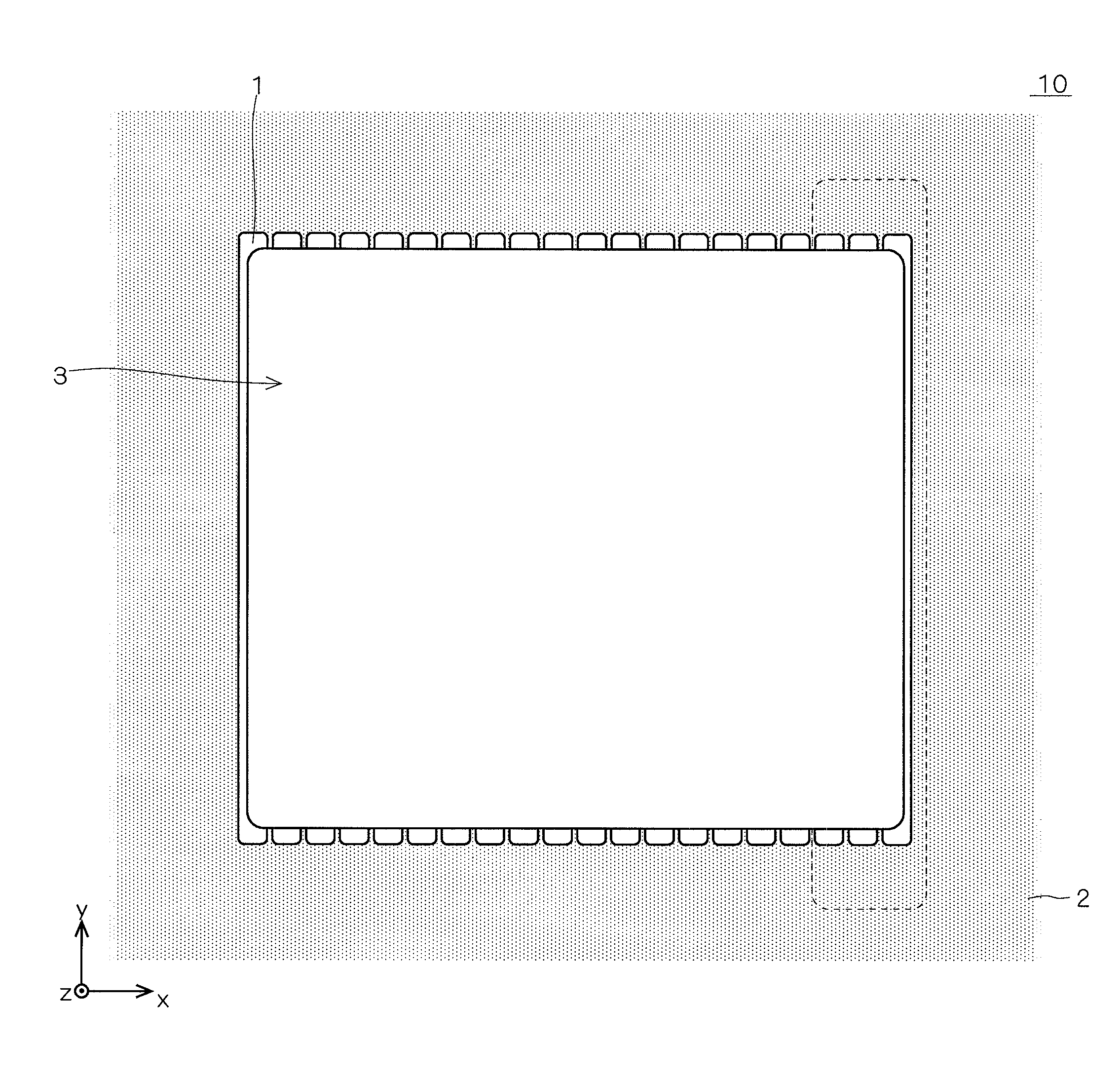
Figure 1 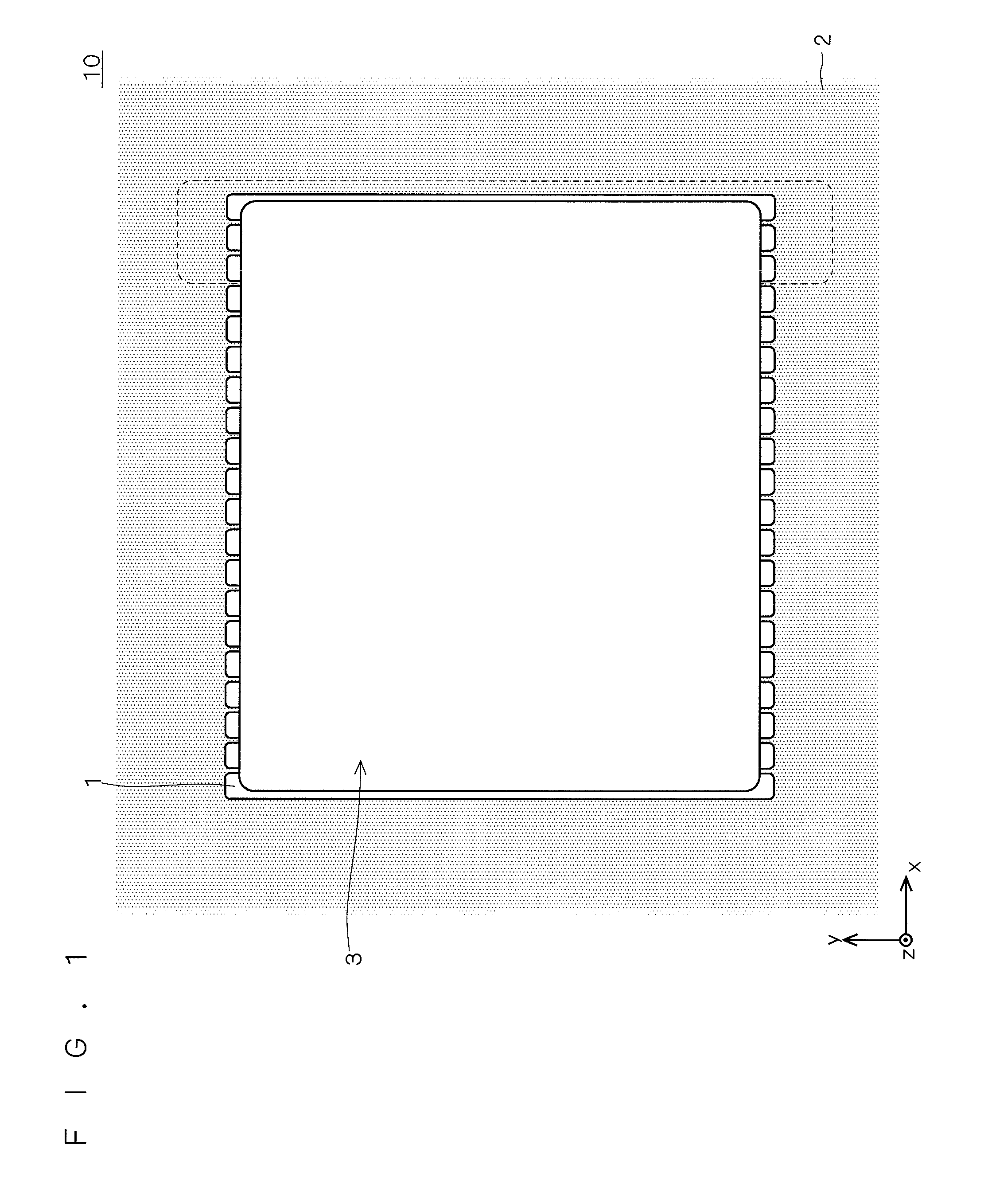
Figure 2 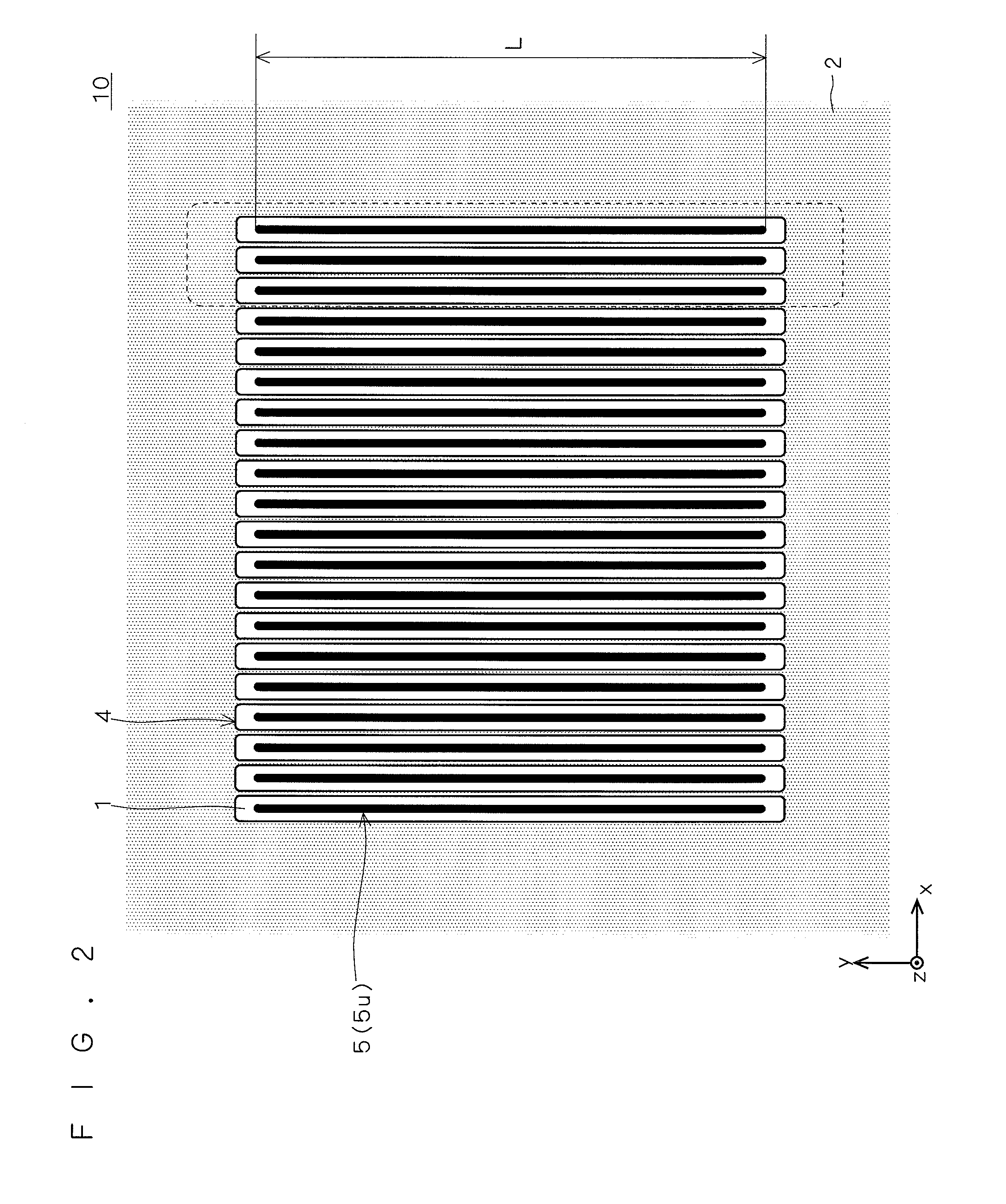
Figure 3
Abstract
Description
FIELD OF THE INVENTION
[0001] The present invention relates to a semiconductor device for power applications, and more particularly to a power inverter or converter circuit device.DESCRIPTION OF THE BACKGROUND ART
[0002] A semiconductor-employed switching device (transistor, thyristor, etc.) or rectifier device (diode) is widely used as a power inverter or converter circuit device. Under the present circumstances, a more compact device with lower losses is preferable for such semiconductor device for power applications in order to meet future demands for higher power. While silicon has conventionally been used widely as a semiconductor material, wide band gap semiconductor materials having higher breakdown fields are being developed as next-generation semiconductor materials in light of the present circumstances. Since what is called wide band gap semiconductor materials such as diamond, SiC, group-III nitride semiconductor, etc. are expected to have low on-state resistance and high bre...
Examples
first preferred embodiment
[0034]Overall Structure of Semiconductor Device FIG. 1 is a top view of a semiconductor device 10 according to a first preferred embodiment of the present invention. As shown in FIG. 1, the semiconductor device 10 schematically includes a conductive layer 1, a cathode portion 2 and an electrode pad layer 3 both provided on the conductive layer 1. More specifically, the semiconductor device 10 has a structure as shown in FIGS. 2 and 3. FIG. 2 is a top view of the semiconductor device 10 with the electrode pad layer 3 omitted, and FIG. 3 is a cross sectional view of part indicated by broken lines in FIG. 1 (a corresponding part in FIG. 2 is also indicated by broken lines). Each part in the respective drawings including FIG. 1 is not always drawn at practical ratio.
[0035]In the semiconductor device 10, the cathode portion 2 is formed substantially on the entire surface of the conductive layer 1 as shown in FIG. 2, but at its central part, a plurality of rectangular hollow regions 4 whe...
second preferred embodiment
[0067]While the first preferred embodiment has described the semiconductor device 10 serving as a P—N junction horizontal diode by forming each unit anode portion 5u to have a two-layered structure of p-type layer 5a and unit anode electrode 5b and creating the P—N junction between the conductive layer 1 and p-type layer 5a, the horizontal diode is not limited to a P—N junction type. The present embodiment will be directed to a semiconductor device 10 serving as a Schottky junction horizontal diode.
[0068]More specifically, a Schottky junction horizontal diode structure is obtained by forming all the unit anode portions 5u to have a Schottky junction with the conductive layer 1 using a predetermined metal, rather than forming each unit anode portion 5u shown in FIGS. 2 and 3 to have a two-layered structure of p-type layer 5a and unit anode electrode 5b as shown in FIG. 4. Such unit anode portion 5u may be made of Ni, for example.
[0069]The semiconductor device 10 having such Schottky ...
third preferred embodiment
[0073]The present embodiment will be directed to a semiconductor device 10 of horizontal diode structure having a P—N junction and a Schottky junction in combination. FIG. 6 is a diagram for explaining the structure of each unit anode portion 5u according to the present embodiment. Such horizontal diode of combined structure is obtained by forming each unit anode portion 5u shown in FIGS. 2 and 3 into the form as shown in FIG. 6, rather than FIG. 4.
[0074]More specifically, each unit anode electrode part 5u includes a p-type layer 5c and a unit anode electrode 5d. The p-type layer 5c is joined to the conductive layer 1 from above at a junction 7a. The p-type layer 5c is a p-type semiconductor layer in which holes are majority carriers, and is formed similarly to the p-type layer 5a according to the first preferred embodiment. The unit anode electrode 5d is provided between the p-type layer 5c and electrode pad layer 3 similarly to the unit anode electrode 5b according to the first pr...