
Method of manufacturing semiconductor device
Patent Information
- Authority / Receiving Office
- US · United States
- Current Assignee / Owner
- Publication Date
- 2019-01-17
Smart Images
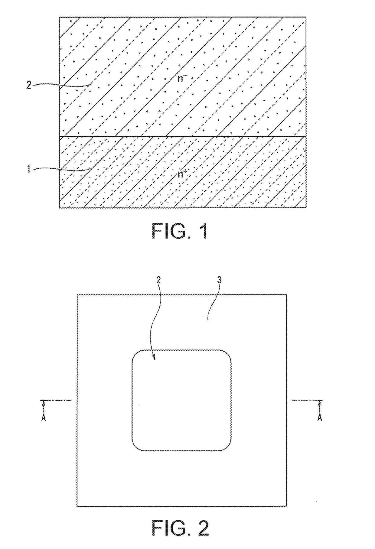
Figure 1 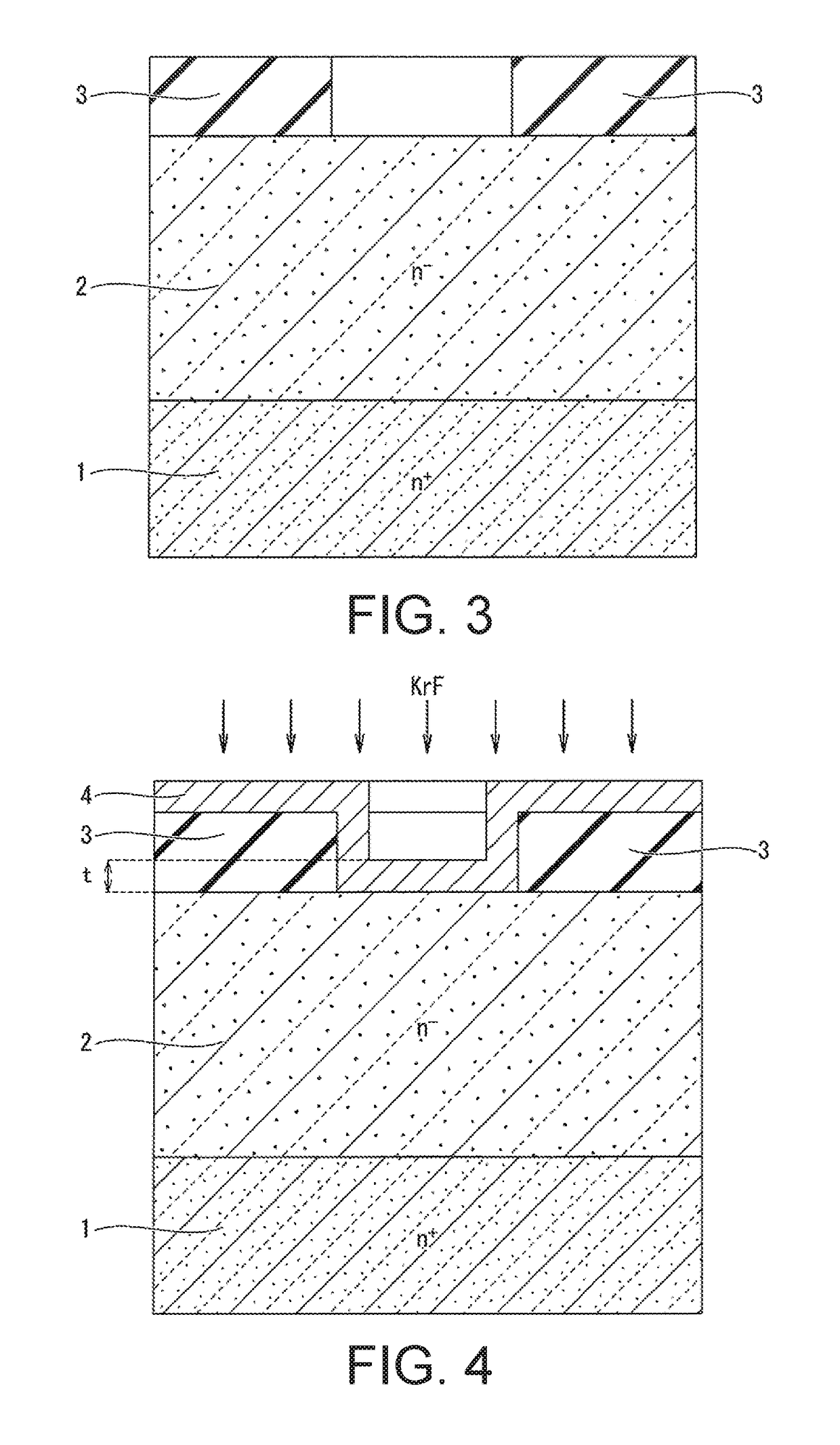
Figure 2 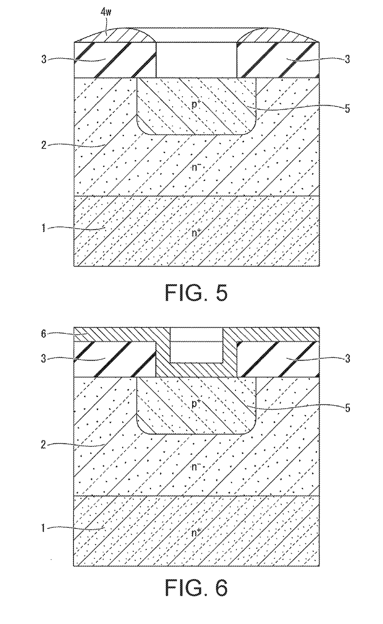
Figure 3
Abstract
Description
BACKGROUND OF THE INVENTIONTechnical Field
[0001] The present invention relates to a method of manufacturing a semiconductor device.Background Art
[0002] Semiconductor devices using silicon carbide (SiC) and more particularly 4H silicon carbide (4H-SiC) have attracted attention as power semiconductors. In 4H-SiC semiconductor devices, first, a crystalline layer of 4H-SiC of a desired impurity concentration is epitaxially grown on a high-impurity concentration (impurity density) n+ 4H-SiC semiconductor substrate, for example. Then, impurity elements are introduced into the crystalline layer of 4H-SiC by implanting ions of an n-type impurity element such as phosphorus (P) or a p-type impurity element such as aluminum (Al) or boron (B) into the (0001) plane or the (000-1) plane of the crystalline layer. Forming impurity-doped layers of the desired conductivity types and impurity concentrations within the crystalline layer makes it possible to manufacture a semiconductor device having the d...
Examples
embodiment 1
[0054]In a method of manufacturing a semiconductor device according to Embodiment 1, a power p-n diode as illustrated in FIG. 8 is manufactured as an SiC semiconductor device. The semiconductor device illustrated in FIG. 8 includes an n-type (n+) supporting layer (SiC substrate) 1 of a high impurity concentration and an n-type (n) to-be-doped layer 2 of a low impurity concentration formed on the upper surface (the silicon (Si) plane) of the supporting layer 1. A p-type (p+) impurity-doped layer 5 of a high impurity concentration is formed in an upper portion of the to-be-doped layer 2.
[0055]To manufacture this semiconductor device, first, as illustrated in FIG. 1, a semiconductor substrate (1, 2) including the n+ supporting layer 1 and the n− to-be-doped layer 2 is prepared. The SiC has a monocrystalline 4H crystal structure, and the overall supporting layer 1 has a thickness sufficient to serve as the lower structure of the semiconductor device to be manufactured thereon. When the ...
modification example 1
[0079]As illustrated in FIG. 14, the method of manufacturing a semiconductor device according to Embodiment 1 can be performed by placing the semiconductor substrate (1, 2) inside an airtight chamber 12 and then using a pump 13 or the like to create a vacuum in the chamber 12. Alternatively, the interior of the chamber 12 may be filled with an inert gas atmosphere. The other steps in the method of manufacturing a semiconductor device according to Modification Example 1 are the same as the respective steps described with reference to FIGS. 1 to 8 and therefore will not be described again here.
[0080]In the method of manufacturing a semiconductor device according to Modification Example 1, performing the laser light irradiation process under vacuum or in an inert gas atmosphere makes it possible to reduce the introduction of oxygen into the surface of the semiconductor substrate (1, 2) caused by heat generated during irradiation with laser light. Therefore, in addition to it being poss...
modification example 2
[0081]Moreover, as illustrated in FIG. 15, after forming the second metal film 7 made of Ni or the like on the bottom surface of the semiconductor substrate (1, 2), the contact electrode connected to the n+ supporting layer 1 may be formed by irradiating the second metal film 7 with high-energy laser light instead of by vacuum-annealing at approximately 1000° C. As illustrated in FIG. 16, irradiating the second metal film 7 with laser light promotes silicidation, which makes it possible to form an Ni silicide ohmic contact electrode 7b. The steps other than forming the ohmic contact electrode on the bottom surface side are the same as the respective steps described with reference to FIGS. 1 to 8 and therefore will not be described again here.
[0082]In the method of manufacturing a semiconductor device according to Modification Example 2, instead of performing a high-temperature vacuum-annealing process at approximately 1000° C., a laser light irradiation process is performed to promo...