Method for improving optical recording media reading signal stability
An optical recording medium, stable technology, applied in optical recording/reproducing/erasing methods, optical recording systems, recording/reproducing by optical methods, etc., can solve problems such as data loss, recording mark changes, etc., to achieve excellent signal The effect of read stability
- Summary
- Abstract
- Description
- Claims
- Application Information
AI Technical Summary
Problems solved by technology
Method used
Image
Examples
Embodiment 1
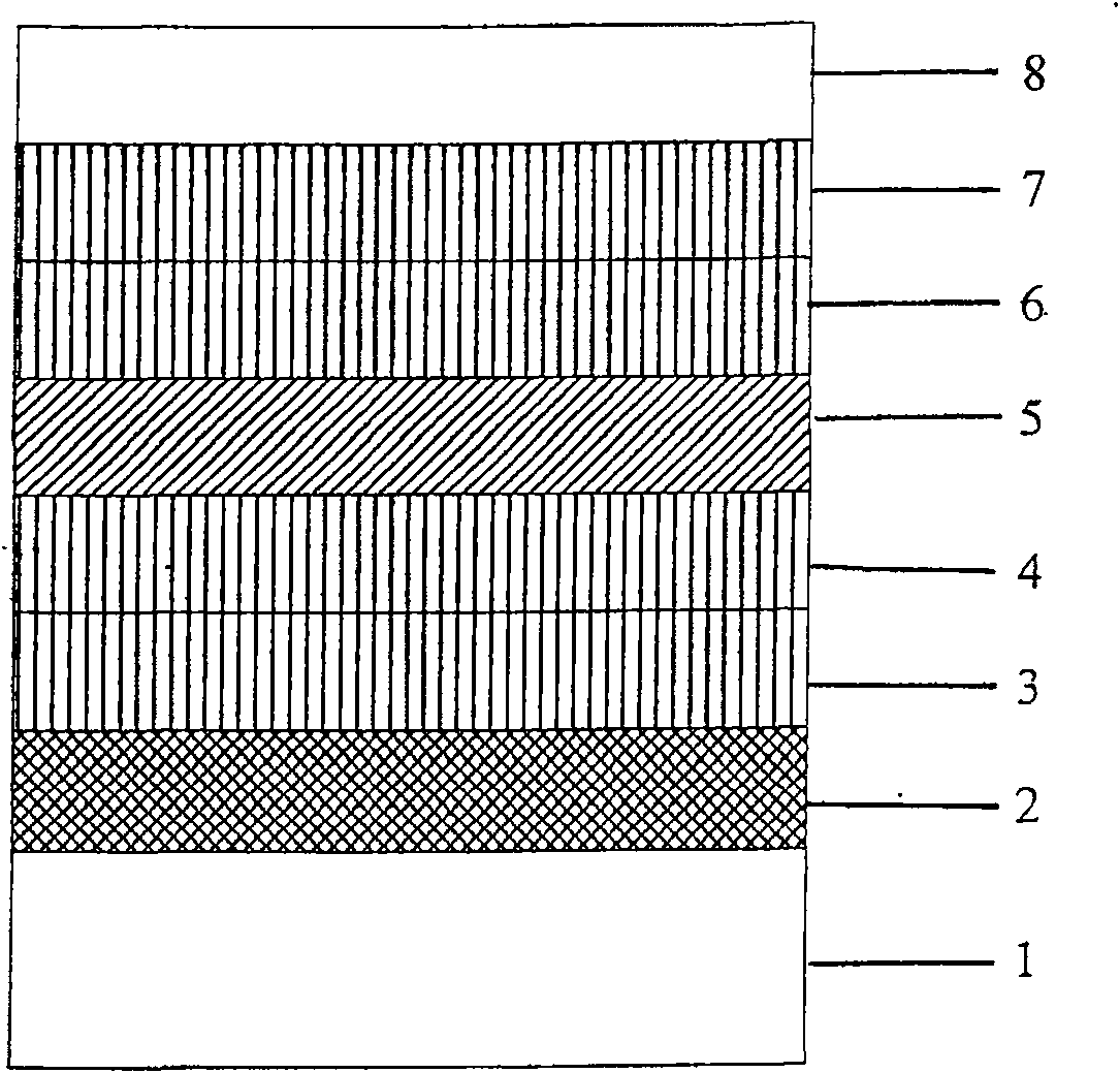
[0033] A Blue-ray Disc-RE substrate (1) with grooves and lands is prepared. The track pitch is 74 μm and the thickness is 1.1 mm. Plating a silver (Ag) reflective layer (2) with a thickness of 100nm on the substrate by magnetron sputtering, and then plating a silicon nitride (SiN) first interface layer (3) with a thickness of 8nm on the reflective layer , and then plate zinc sulfide-silicon oxide (ZnS-SiO) with a thickness of 8nm on the first interface layer 2 ) the first protective layer (4), and then respectively form a recording layer (5) with a thickness of 11nm on the protective layer, and then plate zinc sulfide-silicon oxide (ZnS-SiO2) with a thickness of 19nm on the recording layer. 2) the second protective layer (6), and a second interface layer (7) of silicon nitride (SiN) with a thickness of 30nm is plated on the second protective layer, the film structure diagram is as follows figure 1 shown. Finally, a light-transmitting film (8) with a thickness of 0.1 mm was s...
Embodiment 2
[0042] Prepare a blue-ray disc-recordable disc (Blue-ray Disc-RE) substrate with grooves and lands, the track pitch is 74 μm, and the thickness is 1.1 mm. A silver (Ag) reflective layer with a thickness of 100nm is plated on the substrate by magnetron sputtering, and then a first interface layer of silicon nitride (SiN) with a thickness of 8nm is plated on the reflective layer, and then the first interface layer is coated on the first The interface layer is plated with zinc sulfide-silicon oxide (ZnS-SiO) with a thickness of 8nm 2 ) the first protective layer, and then form a recording layer with a thickness of 13nm on the protective layer, and then plate zinc sulfide-silicon oxide (ZnS-SiO2) with a thickness of 19nm on the recording layer 2 ) a second protective layer, and a second interface layer of silicon nitride (SiN) with a thickness of 30 nm is plated on the second protective layer. Finally, a light-transmitting film with a thickness of 0.1 mm was spin-coated on the pr...
Embodiment 3
[0044] Example 3:
[0045] Prepare a blue-ray disc-recordable disc (Blue-ray Disc-RE) substrate with grooves and lands, the track pitch is 74 μm, and the thickness is 1.1 mm. A silver (Ag) reflective layer with a thickness of 100nm is plated on the substrate by magnetron sputtering, and then a first interface layer of silicon nitride (SiN) with a thickness of 8nm is plated on the reflective layer, and then the first interface layer is coated on the first The interface layer is plated with zinc sulfide-silicon oxide (ZnS-SiO) with a thickness of 8nm 2 ) the first protective layer, and then form a recording layer with a thickness of 15nm on the protective layer, and then plate zinc sulfide-silicon oxide (ZnS-SiO2) with a thickness of 19nm on the recording layer 2 ) a second protective layer, and a second interface layer of silicon nitride (SiN) with a thickness of 30 nm is plated on the second protective layer. Finally, a light-transmitting film with a thickness of 0.1 mm was ...
PUM
| Property | Measurement | Unit |
|---|---|---|
| thickness | aaaaa | aaaaa |
| thickness | aaaaa | aaaaa |
| thickness | aaaaa | aaaaa |
Abstract
Description
Claims
Application Information
 - R&D Engineer
- R&D Manager
- IP Professional
- Industry Leading Data Capabilities
- Powerful AI technology
- Patent DNA Extraction
Browse by: Latest US Patents, China's latest patents, Technical Efficacy Thesaurus, Application Domain, Technology Topic, Popular Technical Reports.
© 2024 PatSnap. All rights reserved.Legal|Privacy policy|Modern Slavery Act Transparency Statement|Sitemap|About US| Contact US: help@patsnap.com


