Method for improving optical recording media reading signal stability
An optical recording medium, a stable technology, applied in optical recording/reproduction/erasing methods, optical recording systems, recording/reproduction with optical methods, etc., can solve problems such as data loss, recording mark changes, etc., and achieve excellent signals The effect of reading stability
- Summary
- Abstract
- Description
- Claims
- Application Information
AI Technical Summary
Problems solved by technology
Method used
Image
Examples
Embodiment 1
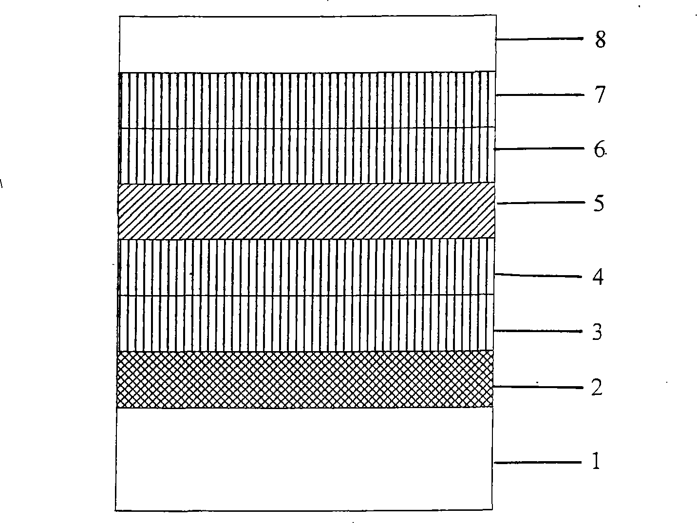
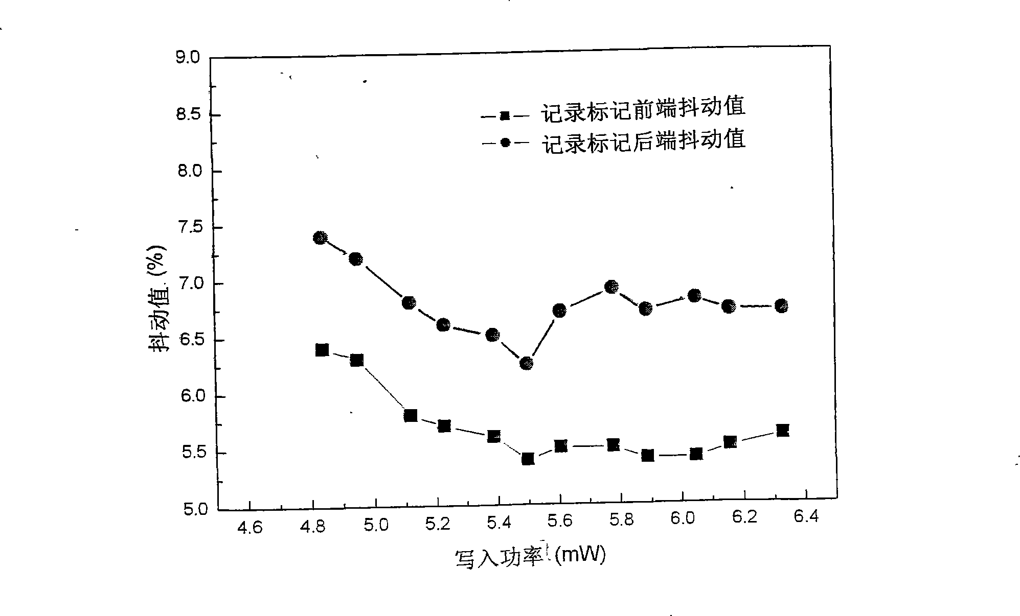
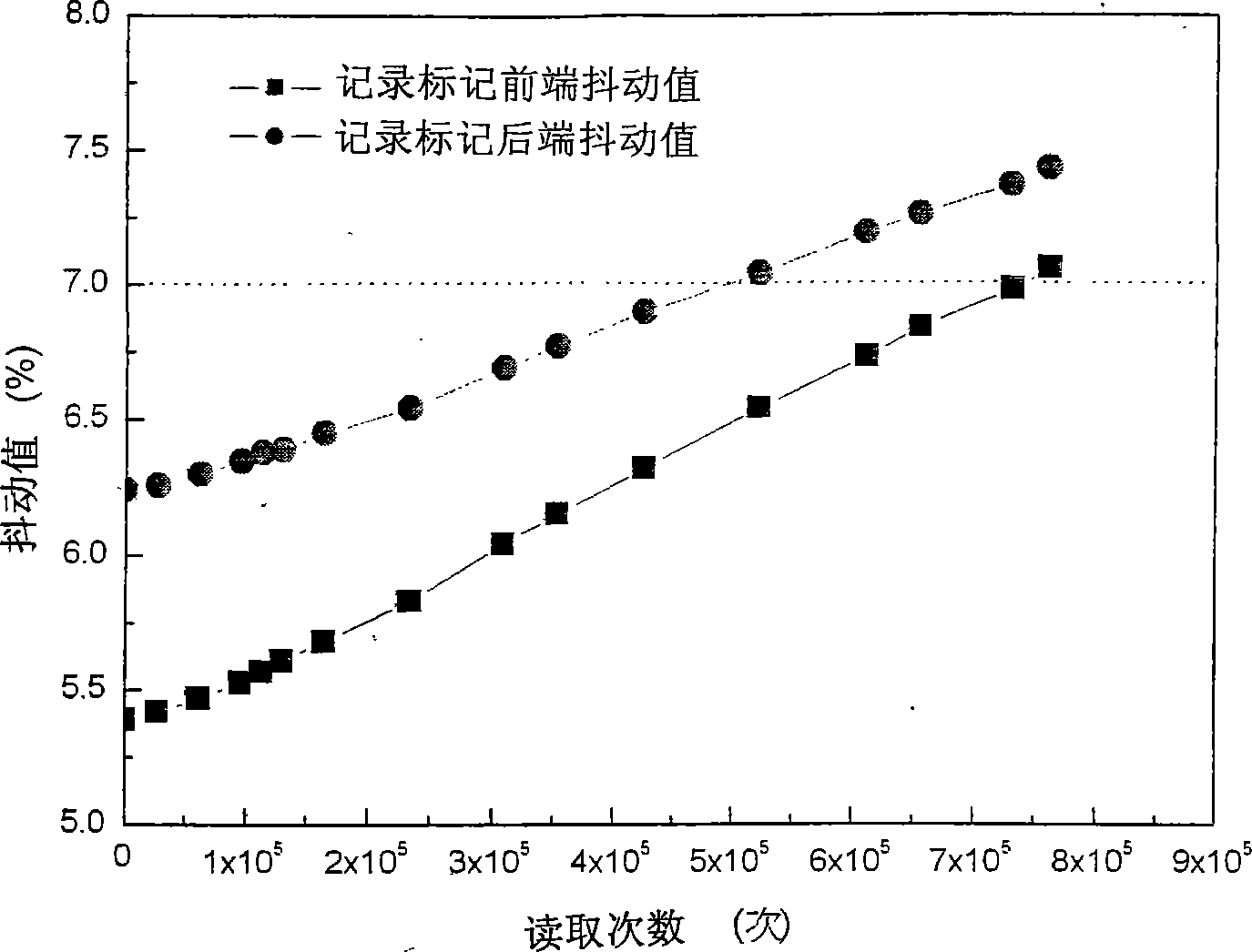
[0033] A Blue-ray Disc-RE substrate (1) with grooves and lands is prepared. The track pitch is 74 μm and the thickness is 1.1 mm. Plating a silver (Ag) reflective layer (2) with a thickness of 100nm on the substrate by magnetron sputtering, and then plating a silicon nitride (SiN) first interface layer (3) with a thickness of 8nm on the reflective layer , and then plate zinc sulfide-silicon oxide (ZnS-SiO) with a thickness of 8nm on the first interface layer 2) the first protective layer (4), and then respectively form a recording layer (5) with a thickness of 11nm on the protective layer, and then plate zinc sulfide-silicon oxide (ZnS-SiO2) with a thickness of 19nm on the recording layer. 2 ) the second protective layer (6), and a second interface layer (7) of silicon nitride (SiN) with a thickness of 30nm is plated on the second protective layer, the film structure diagram is as follows figure 1 shown. Finally, a light-transmitting film (8) with a thickness of 0.1 mm was s...
Embodiment 2
[0042] Prepare a blue-ray disc-recordable disc (Blue-ray Disc-RE) substrate with grooves and lands, the track pitch is 74 μm, and the thickness is 1.1 mm. A silver (Ag) reflective layer with a thickness of 100nm is plated on the substrate by magnetron sputtering, and then a first interface layer of silicon nitride (SiN) with a thickness of 8nm is plated on the reflective layer, and then the first interface layer is coated on the first The interface layer is plated with zinc sulfide silicon oxide (ZnS-SiO) with a thickness of 8nm 2 ) the first protective layer, and then form a recording layer with a thickness of 13nm on the protective layer, and then plate zinc sulfide-silicon oxide (ZnS-SiO2) with a thickness of 19nm on the recording layer 2 ) a second protective layer, and a second interface layer of silicon nitride (SiN) with a thickness of 30 nm is plated on the second protective layer. Finally, a light-transmitting film with a thickness of 0.1 mm was spin-coated on the pr...
Embodiment 3
[0044] Example 3:
[0045] Prepare a blue-ray disc-recordable disc (Blue-ray Disc-RE) substrate with grooves and lands, the track pitch is 74 μm, and the thickness is 1.1 mm. A silver (Ag) reflective layer with a thickness of 100nm is plated on the substrate by magnetron sputtering, and then a first interface layer of silicon nitride (SiN) with a thickness of 8nm is plated on the reflective layer, and then the first interface layer is coated on the first The interface layer is plated with zinc sulfide-silicon oxide (ZnS-SiO) with a thickness of 8nm 2 ) the first protective layer, and then form a recording layer with a thickness of 15nm on the protective layer, and then plate zinc sulfide silicon oxide (ZnS-SiO 2 ) a second protective layer, and a second interface layer of silicon nitride (SiN) with a thickness of 30 nm is plated on the second protective layer. Finally, a light-transmitting film with a thickness of 0.1 mm was spin-coated on the protective layer as the light-t...
PUM
| Property | Measurement | Unit |
|---|---|---|
| Thickness | aaaaa | aaaaa |
Abstract
Description
Claims
Application Information
 - R&D Engineer
- R&D Manager
- IP Professional
- Industry Leading Data Capabilities
- Powerful AI technology
- Patent DNA Extraction
Browse by: Latest US Patents, China's latest patents, Technical Efficacy Thesaurus, Application Domain, Technology Topic, Popular Technical Reports.
© 2024 PatSnap. All rights reserved.Legal|Privacy policy|Modern Slavery Act Transparency Statement|Sitemap|About US| Contact US: help@patsnap.com


