Printing circuit board and method for testing anisotropic conducting membrance
A technology of anisotropic conductive film and printed circuit board, which is applied in the direction of printed circuit, measuring device, optical test defect/defect, etc. connected with non-printed electrical components, which can solve the problem that the detection of anisotropic conductive adhesive cannot be correctly judged, etc. question
- Summary
- Abstract
- Description
- Claims
- Application Information
AI Technical Summary
Problems solved by technology
Method used
Image

Examples
Embodiment Construction
[0017] Specific embodiments are given below to describe the content of the present invention in detail, and the accompanying drawings are used as auxiliary descriptions.
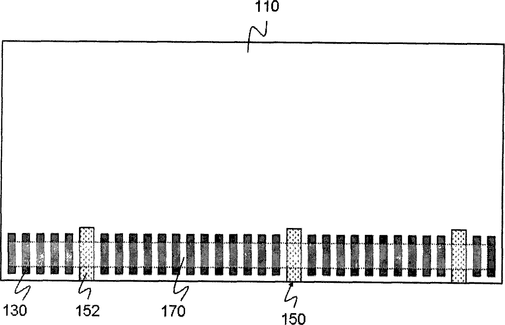
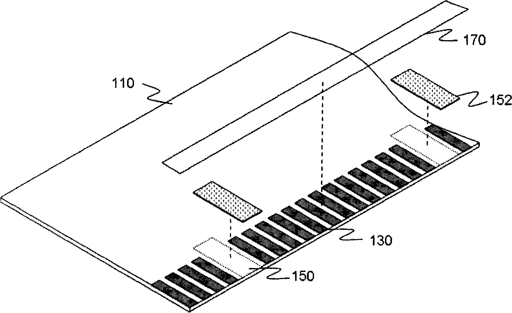
[0018] Figure 1A and 1B It is a schematic diagram of the printed circuit board of the present invention, and the printed circuit board includes: a substrate 110 , a conductive terminal (lead) 130 , a detection area 150 and a pigment coating 152 .
[0019] The conductive terminals 130 are arranged in a row on the substrate 110 , and one or more detection regions 150 are disposed between the conductive terminals 130 , and the detection regions 150 are covered with a pigment coating 152 .
[0020] Among them, the pigment coating 152 is preferably a paint with stable color; more precisely, the pigment coating 152 is not easily affected by environmental conditions (eg, temperature, humidity, etc.). In a preferred embodiment, the pigment coating 152 is resistant to chemical solvents, especially commonly used che...
PUM
 Abstract
Description
Claims
Application Information
 - R&D Engineer
- R&D Manager
- IP Professional
- Industry Leading Data Capabilities
- Powerful AI technology
- Patent DNA Extraction
Browse by: Latest US Patents, China's latest patents, Technical Efficacy Thesaurus, Application Domain, Technology Topic.
© 2024 PatSnap. All rights reserved.Legal|Privacy policy|Modern Slavery Act Transparency Statement|Sitemap