

Semiconductor device
A semiconductor and internal wire technology, applied in the direction of semiconductor devices, semiconductor/solid-state device components, electric solid-state devices, etc., can solve the problems of hindering the flow of resin, difficult to inject resin, etc.
- Summary
- Abstract
- Description
- Claims
- Application Information
AI Technical Summary
Problems solved by technology
Method used
Image

Examples
Embodiment approach 1
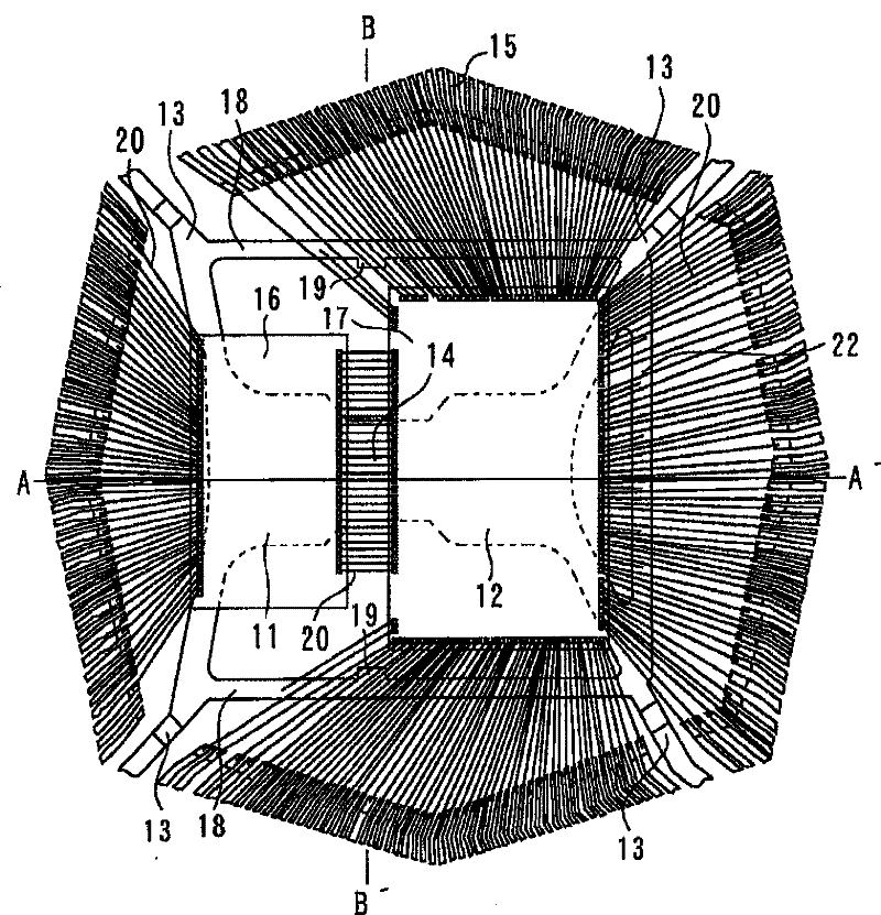
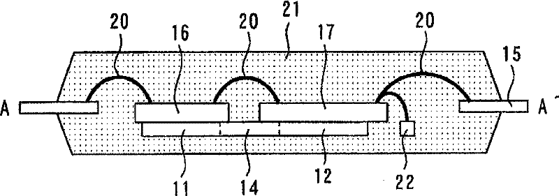
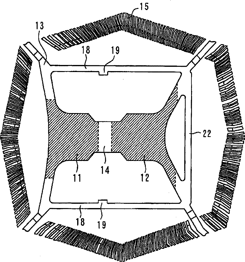
[0027] figure 1 is a plan view showing the inside of a semiconductor device according to an embodiment of the present invention, figure 2 yes figure 1 Cross-sectional view of A-A′. Figure 10 yes figure 1 Cross-sectional view of B-B′. The first lower backing plate 11 (first portion) and the second lower backing plate 12 (second portion) are arranged side by side. The first and second lower backing plates 11 , 12 are supported by suspension wires 13 , and both are connected by connecting wires 14 . The first and second lower backing plates 11, 12, the connection lead 14, and the suspension lead 13 constitute a metal mounting member in which metal parts are integrally molded. A plurality of inner leads 15 are arranged around the first and second lower backing plates 11 and 12 .
[0028] The first chip 16 has its principal surface overlapped with the first lower substrate 11 and is mounted on the principal surface of the first lower substrate 11 with paste (not shown). ...
Embodiment approach 2
[0052] In this Embodiment 2, if Figure 7As shown, instead of providing markings on the horizontal bars 18 as in the first embodiment, recesses 24 are provided as markings on the connection leads 14 . That is, the mounting member has a connecting wire 14 (third portion) that is located between the first and second chips 16, 17 and that connects the first underlayment 11 (first portion) and the second underlayment 12 (second portion). . Further, on the side surface continuous from the first lower backing plate 11 to the second lower backing plate 12 via the connecting lead 14 , a concave portion 24 dented toward the inner side of the side surface is provided. The bottom part of the recess 24 lies at least on the connecting wire 14 . and, if Figure 8 As shown, the first and second chips 16 , 17 are mounted on the lower pads 11 , 12 . Other structures are the same as those in Embodiment 1. In this way, when the chips 16 and 17 are mounted on the lower substrate, the first a...
PUM
 Abstract
Description
Claims
Application Information