Optical waveguide device system

An optical waveguide and device technology, applied in the field of optical waveguide device systems, can solve the problems of increasing the weight and volume of the optical system, and achieve the effects of weight reduction, small size and compact structure

Active Publication Date: 2013-12-04
UNIV OF SHANGHAI FOR SCI & TECH
View PDF3 Cites 20 Cited by
  • Summary
  • Abstract
  • Description
  • Claims
  • Application Information

AI Technical Summary

Problems solved by technology

Although a large field of view can be obtained by conventional imaging methods, with the increase of th

Method used


Image

  • Optical waveguide device system
  • Optical waveguide device system
  • Optical waveguide device system

Examples


Embodiment Construction

[0016] The optical waveguide device system of the preferred embodiment of the present invention will be described in detail below with reference to the accompanying drawings. Those skilled in the art should understand that the embodiments described below are only illustrative illustrations of the present invention, and are not intended to limit it in any way.

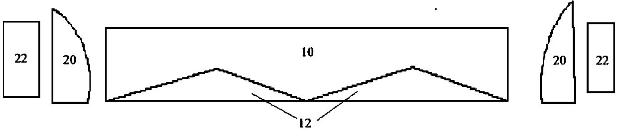
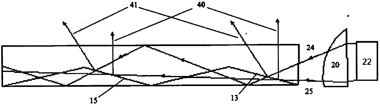
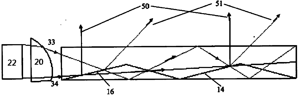
[0017] Such as figure 1 As shown, the optical waveguide device system according to a preferred embodiment of the present invention includes: a light wave transmission substrate 10 , a light wave outcoupling element 12 , a display light source 22 , and a collimator lens 20 .

[0018] The display light source 22 may be composed of current mainstream display light sources such as CRT, OLED, and LCD. The display light source mainly provides image light waves for display. Since different light sources have different polarization states, in order to avoid undesired phenomena such as ghosting when light waves are transmitted...


PUM


Abstract

The invention discloses an optical waveguide device system which comprises display light sources, collimating lenses, an optical transmission substrate and optical wave coupling and outputting elements. The display light sources are used for providing optical waves of displayed images; the collimating lenses are used for collimating the optical waves from the light sources; the collimated optical waves enter the optical transmission substrate and are transmitted according to preset paths, transverse grooves are formed in the bottom of the optical transmission substrate, and the cross sections of the grooves in the longitudinal direction of the substrate are triangular and keep unchanged in the longitudinal directions of the grooves; the optical wave coupling and outputting elements are provided with upward triangular protrusions, the protrusions can be matched with the grooves, film layers are arranged on two side surfaces of each protrusion, and the two side surfaces with the film layers of each protrusion are adhered onto side surfaces of the corresponding grooves, so that light can be coupled and outputted to the optical transmission substrate via the side surfaces with the film layers of the protrusions, large-angle incident light rays can be selectively transmitted via the film layers, and the transmittance of small-angle incident light rays can be improved. Compared with the prior art, the optical waveguide device system has the advantages of large field of view, compact structure, portability and small size.

Description

technical field [0001] The invention relates to an optical waveguide device system, in particular to an optical waveguide device system which can be used for miniature image display. Background technique [0002] Head-mounted video devices and other compact display systems, flat panel displays, notebooks, etc. usually rely on optical components to transmit the image to be displayed. For example, the display system displays images in front of human eyes through transparent lenses, so that the image information in the lenses can be browsed while observing the environment ahead through the lenses. Usually, the core optical system of this type of display is mainly composed of three parts: a light wave coupling input device, a light wave transmission substrate, and a light wave output coupling device. At the same time, lightweight, compact, large field of view and high resolution images have always been the pursuit of this type of optical system. Although a large field of view ...

Claims


Application Information

Patent Timeline
IPC IPC(8): G02B6/122
Inventor 张文君许键
Owner UNIV OF SHANGHAI FOR SCI & TECH
Why Eureka
Try Eureka