Supercharge Your Innovation With Domain-Expert AI Agents!

Photodetector and manufacturing method thereof

A photodetector and photocurrent technology, applied in the field of photodetectors, can solve the problem of crosstalk of photosensitive pixel elements and other problems

Active Publication Date: 2016-03-30
INFINEON TECH AG
View PDF4 Cites 0 Cited by
  • Summary
  • Abstract
  • Description
  • Claims
  • Application Information

AI Technical Summary

Problems solved by technology

[0006] Crosstalk between two or more photosensitive pixel elements can be a problem when several photosensitive pixel elements are arranged in an array

Method used


Image

  • Photodetector and manufacturing method thereof
  • Photodetector and manufacturing method thereof
  • Photodetector and manufacturing method thereof

Examples


Embodiment Construction

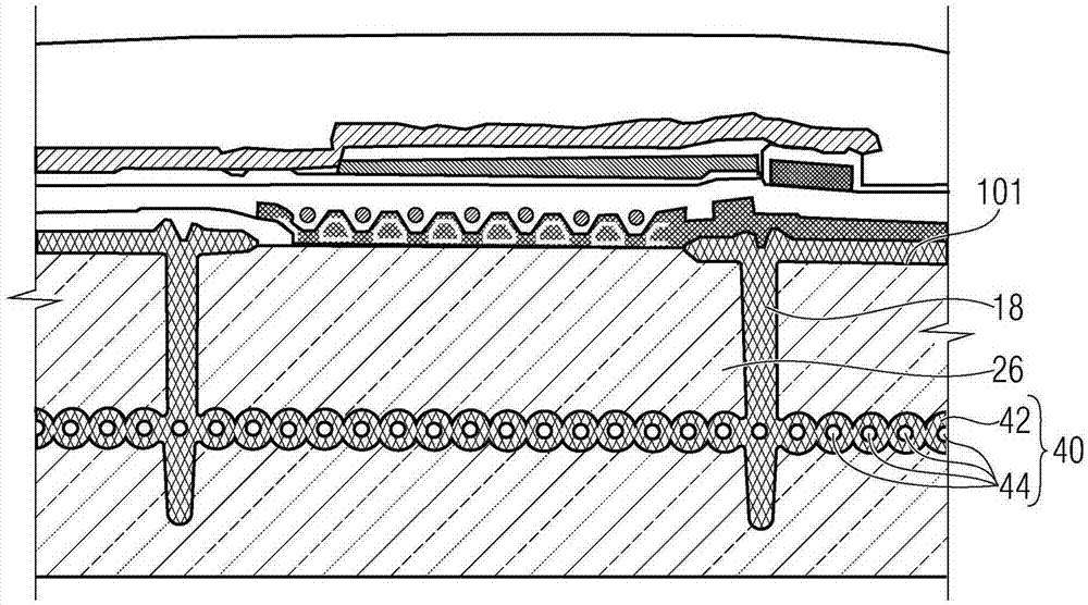
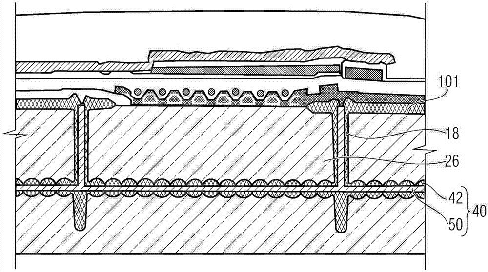
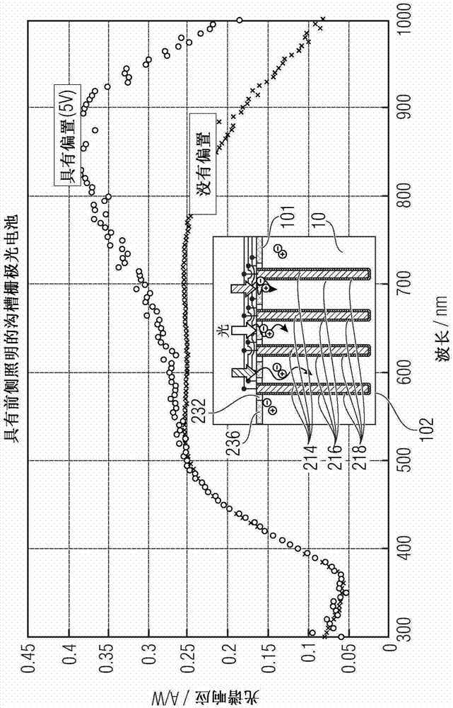
[0032] Before describing the embodiments of the present invention in detail below using the accompanying drawings, it will be noted that the same or similar reference numerals are provided to the same element (or elements) having the same function and the same or similar reference numerals are generally omitted. Repeated descriptions of elements. Descriptions of elements with the same or similar reference numerals are mutually interchangeable. In the following description, numerous details are set forth in order to provide a more complete explanation of embodiments of the invention. It will be apparent, however, to one skilled in the art that embodiments of the invention may be practiced without these specific details. In other instances, well-known structures and devices are shown in block diagram form, rather than in detail, in order not to obscure the embodiments of the invention. In other instances, well-known structures and devices are shown in schematic cross-sectional...


PUM


Abstract

The invention discloses a photoelectric detector and a manufacturing method thereof. The photoelectric detector comprises a substrate and an insulating device formed in the substrate. The insulating device is electrically insulated with a constraint region on the substrate. The constraint region is configured to response to irradiation and generates free charge carriers. The photoelectric detector also comprises a reading electrode device providing light current. The light current is formed by at least a part of the free charge carriers which are generated by responding to irradiation. The photoelectric detector also comprises a bias electrode device which is electrically insulated with the constraint region through the insulating device. The bias electrode device is configured to influence space charge carrier distribution in the constraint region, so that compared with a non-bias status, fewer free charge carriers combine on boundaries of the constraint region.

Description

[0001] Cross References to Related Applications [0002] This application is a continuation-in-part of Application Serial No. 13 / 232,564, filed September 14,2011. technical field [0003] Embodiments of the present invention relate to a photodetector. A further embodiment of the invention relates to a method for manufacturing a photodetector. Further embodiments relate to arrays of photodetectors or light sensitive pixel elements. Furthermore, some embodiments of the invention relate to a photosensitive pixel element. Background technique [0004] In many industrial and consumer applications, there is a need to analyze optical data and images. There is a trend towards highly integrated photosensitive pixel arrays (image pickup elements) integrated in CMOS (Complementary Metal Oxide Semiconductor) circuits or ASICs (Application Specific Integrated Circuits). [0005] These devices can be used eg in security applications, IT (Information Technology) products and optical co...

Claims


Application Information

Patent Timeline
Patent Type & Authority Patents(China)
IPC IPC(8): H01L31/112H01L31/0352H01L31/18
CPCH01L31/062Y02E10/50Y02P70/50
Inventor 托拉尔夫·考奇
Owner INFINEON TECH AG
Features
  • R&D
  • Intellectual Property
  • Life Sciences
  • Materials
  • Tech Scout
  • Unparalleled Data Quality
  • Higher Quality Content
  • 60% Fewer Hallucinations
Learn More