PCB design method for inhibiting plane resonance

A design method and plane technology, applied in the field of electronics, can solve the problems of increasing the difficulty of PCB design and increasing the design cost, and achieve the effect of reducing the ground bounce effect, reducing the design cost and improving the resonance.

Active Publication Date: 2014-09-03
LANGCHAO ELECTRONIC INFORMATION IND CO LTD
View PDF3 Cites 1 Cited by
  • Summary
  • Abstract
  • Description
  • Claims
  • Application Information

AI Technical Summary

Problems solved by technology

[0006] However, the method of adding decoupling capacitors will increase the design cost, and when the PCB design is getting more and more dense, adding capacitors will increase the difficulty of PCB design

Method used


Image

  • PCB design method for inhibiting plane resonance
  • PCB design method for inhibiting plane resonance

Examples


Embodiment 1

[0019] A PCB design method to suppress plane resonance In the design of printed circuit boards, the method of changing the plane cutting is used to change the cavity formed between the power layer and the ground layer (or the power layer and the power layer), thereby improving the frequency band we focus on. resonance.

Embodiment 2

[0021] On the basis of Embodiment 1, the method of changing the plane cutting described in this embodiment is that if a resonant frequency point with the same frequency as the signal in the wiring area appears in a certain area, the power layer adjacent to this area is hollowed out for design , the hollowed-out area has the same size as the resonance area.

Embodiment 3

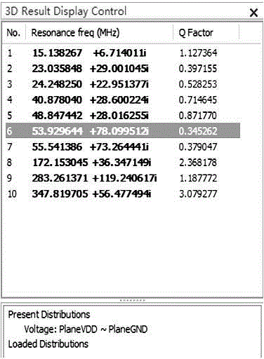
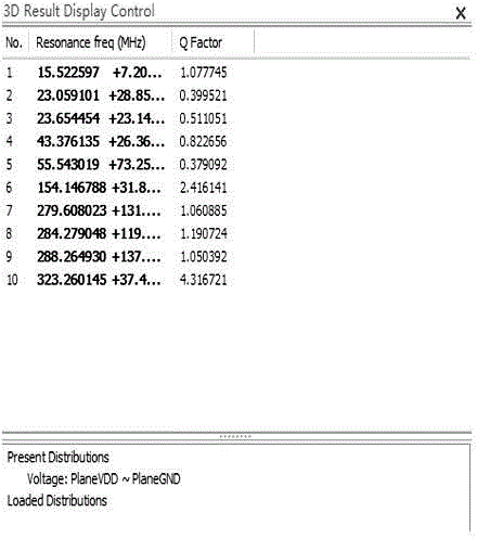
[0023] On the basis of Embodiment 1 or 2, in this embodiment, the frequency point resonance distribution of the planar resonator can be viewed through the SIGRITY POWER SI simulation software.


PUM


Abstract

The invention discloses a PCB (Printed Circuit Board) design method for inhibiting plane resonance. According to the design of the PCB, a cavity formed by a power supply layer and a ground layer (or power supply layers) is changed by use of a method of changing plane cutting, so that the resonance of a frequency band concerned by people is improved. The PCB design method is capable of reducing the ground bounce effect caused by plane intrinsic resonance; the resonance condition of the concerned frequency band can be avoided by use of a method of changing plane design; the concerned frequency band is prevented from generating the plane resonance, electromagnetic radiation caused by resonance is avoided, and signal completeness and power completeness are guaranteed.

Description

technical field [0001] The invention relates to the field of electronics, to PCB design software, to the field of SIGRITY POWER SI simulation software, and in particular to a PCB design method for suppressing plane resonance. technical background [0002] In the FPGA design process, due to the high density of electronic components on the PCB, the denser wiring, and the higher and higher signal frequencies, EMC (electromagnetic compatibility) and EMI (electromagnetic interference) problems inevitably occur. [0003] At present, in the design of printed circuit boards, the power supply layer and the ground layer form a planar resonant cavity, and there are some resonant frequency points in certain areas in the planar resonant cavity. [0004] If there is exactly the same frequency excitation source or signal line in the area where the resonance frequency appears in the printed circuit board design, it will cause the plane to resonate at this frequency. This creates electromag...

Claims


Application Information

Patent Timeline
Patent Type & Authority Applications(China)
IPC IPC(8): G06F17/50
Inventor 宋明哲范晓丽
Owner LANGCHAO ELECTRONIC INFORMATION IND CO LTD
Why Eureka
Try Eureka