

A kind of preparation method of power diode
A technology of power diodes and silicon dioxide, applied in semiconductor/solid-state device manufacturing, electrical components, circuits, etc., can solve the problems of high cost, time-consuming, low efficiency, etc., to improve the withstand voltage level and reduce the forward turn-on voltage, the effect of improving the withstand voltage of the device
- Summary
- Abstract
- Description
- Claims
- Application Information
AI Technical Summary
Problems solved by technology
Method used
Image

Examples
Embodiment Construction
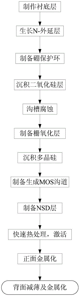
[0048] The principles and features of the present invention are described below in conjunction with the accompanying drawings, and the examples given are only used to explain the present invention, and are not intended to limit the scope of the present invention.
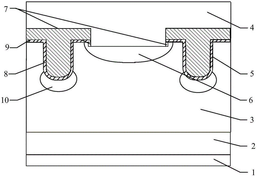
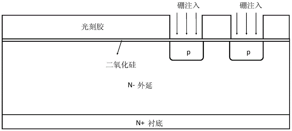
[0049] Such as figure 1 As shown, a power diode according to the present invention comprises a bottom electrode 1, a substrate layer 2, an N-type epitaxial layer 3 and a top electrode 4 from bottom to top, the top electrode 4 is the anode of the power diode, and the bottom electrode 1 is the negative pole of the power diode; wherein at least two grooves 5 are arranged laterally on the upper part of the N-type epitaxial layer 3, and between the N-type epitaxial layer 3 and the top electrode 4 between two adjacent grooves 5 pbody area 6;
[0050] The cross-section of the pbody region 6 is in a "concave" shape with an arc at the bottom, wherein the two convex parts on the upper part of the "concave" shape are the edge...
PUM
 Abstract
Description
Claims
Application Information