A trench type semiconductor power device terminal protection structure and power device

A terminal protection structure and power device technology, applied in semiconductor devices, electrical components, circuits, etc., can solve the problems of weakening the withstand voltage capacity of the terminal protection structure and increasing the electric field intensity of the side wall of the oxide layer, so as to achieve the reduction of potential influence, Effects of increased cost and improved reverse withstand voltage capability

Active Publication Date: 2021-04-06
SOUTHEAST UNIV
View PDF3 Cites 0 Cited by
  • Summary
  • Abstract
  • Description
  • Claims
  • Application Information

AI Technical Summary

Problems solved by technology

However, there are certain defects in this traditional structure. Since the semiconductor well region is offset against the sidewalls of the oxide layer of the voltage divider rings on both sides in the horizontal direction, the potentials of adjacent voltage divider rings will affect each other, and finally the sidewalls of the oxide layer The electric field strength increases, which weakens the withstand voltage capability of the terminal protection structure

Method used


Image

  • A trench type semiconductor power device terminal protection structure and power device
  • A trench type semiconductor power device terminal protection structure and power device
  • A trench type semiconductor power device terminal protection structure and power device

Examples


Embodiment 1

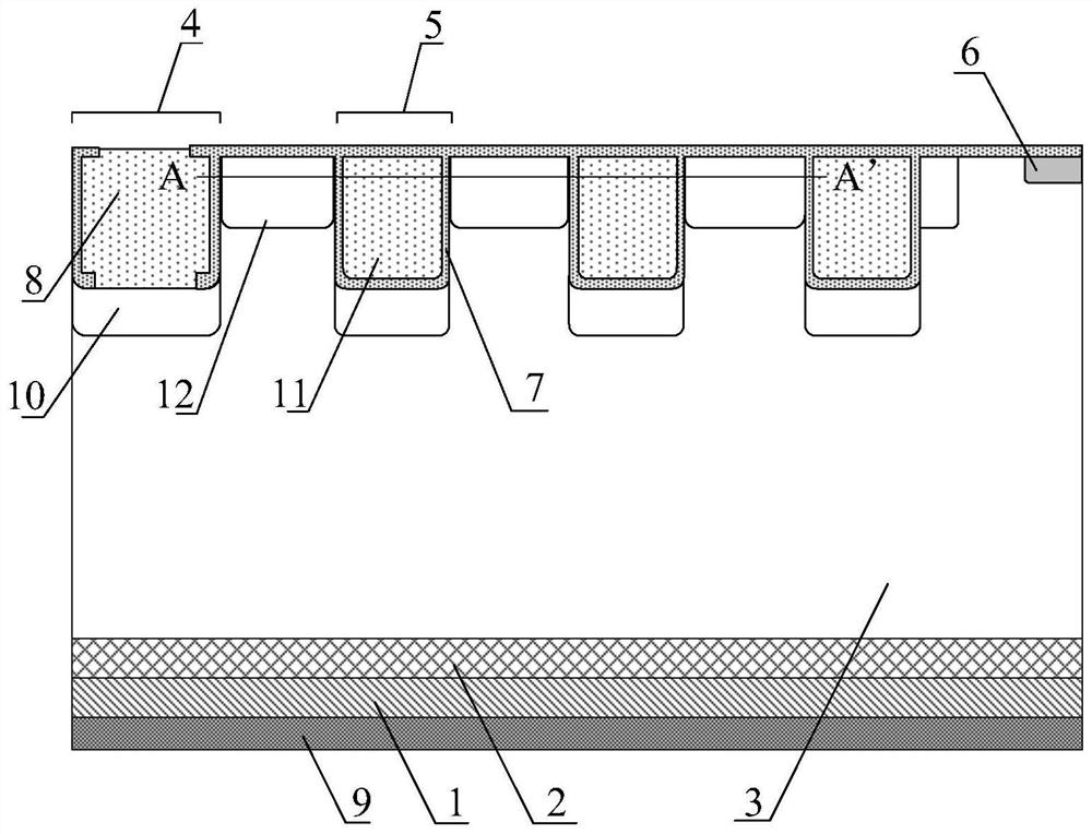
[0026]A trench-type semiconductor power device terminal protection structure, comprising: a first conductivity type substrate 1, a first conductivity type buffer layer 2 is provided on the first conductivity type substrate 1, and a first conductivity type buffer layer 2 is disposed on the first conductivity type buffer layer 2 A drift region 3 of the first conductivity type is provided, a primitive cell region 19 is arranged in the drift region 3 of the first conductivity type, a main voltage divider ring 4 is arranged outside the primitive cell region 19, and at least A sub-voltage divider ring 5, a cut-off ring 6 of the first conductivity type is provided outside the outermost sub-voltage divider ring 5, and a second conductivity type is provided under the main voltage divider ring 4 and each sub-voltage divider ring 5 respectively. The shielding protection layer 10 is covered with an oxide layer on the surface of the drift region 3 of the first conductivity type, between the...

Embodiment 2

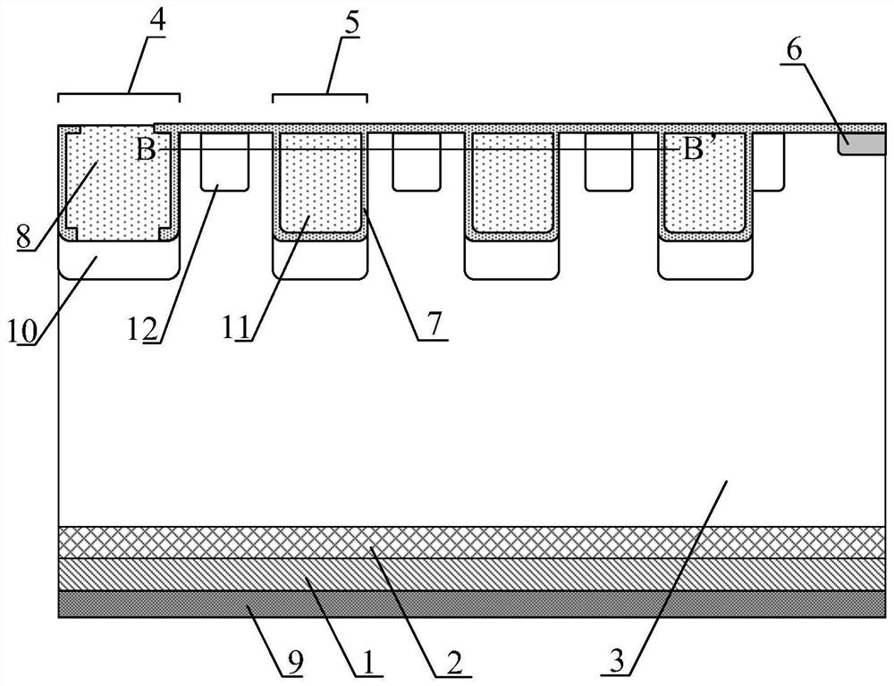
[0028] Embodiment 2 differs from Embodiment 1 only in the position of the well region 12 of the second conductivity type, namely: the second conductive well region 12 located between the main voltage divider ring 4 and the secondary voltage divider ring 5 adjacent to the main voltage divider ring 4 The type well region 12 and the sub-voltage divider ring 5 therein are isolated by the first conductivity type drift region 3, and the second conductivity type well region 12 located between adjacent sub-voltage divider rings 5 ​​is isolated from the adjacent sub-voltage divider ring 5 The outer secondary voltage divider rings 5 ​​are isolated by the drift region 3 of the first conductivity type.

Embodiment 3

[0030] A trench type semiconductor power device, comprising: a trench type semiconductor power device terminal protection structure, the trench type semiconductor power device terminal protection structure comprising: a first conductivity type substrate 1, a first conductivity type substrate 1 The buffer layer 2 of the first conductivity type is provided on it, the drift region 3 of the first conductivity type is arranged on the buffer layer 2 of the first conductivity type, and the original cell region 19 is arranged in the drift region 3 of the first conductivity type, and the original cell region 19 A main voltage divider ring 4 is provided on the outside of the main voltage divider ring 4, and at least one secondary voltage divider ring 5 is provided outside the main voltage divider ring 4, and a first conductivity type cut-off ring 6 is provided outside the outermost secondary voltage divider ring 5. The second conductive type shielding protection layer 10 is respectively ...


PUM

PropertyMeasurementUnit
thicknessaaaaaaaaaa

Abstract

A trench type semiconductor power device terminal protection structure and power device, the power device structure includes a first conductivity type substrate, a first conductivity type buffer layer, a first conductivity type drift region, and in the first conductivity type drift region There is a primary cell area and a terminal protection area, and a main voltage divider ring, a secondary voltage divider ring, and a first conductivity type cut-off ring are provided outside the primary cell area, and a second conductivity type shielding protection layer is provided under the voltage divider ring. The structural feature is that a well region of the second conductivity type is provided between adjacent voltage divider rings, and each voltage divider ring is isolated from the well region of the second conductivity type by a drift region of the first conductivity type. At the same time as the best layer assists in withstand voltage, it can avoid the potential influence between adjacent voltage divider rings, effectively reduce the electric field strength in the voltage divider epoxy layer, and improve the withstand voltage capability of the terminal protection structure, and the structure is compatible with The original manufacturing process is compatible, and the overall performance of the device is improved while keeping the cost unchanged.

Description

technical field [0001] The invention belongs to the technical field of structure design and manufacture of power semiconductor devices. Specifically, the invention mainly relates to a trench type semiconductor power device terminal protection structure and the design and manufacture of power devices. Background technique [0002] The terminal of a power semiconductor device plays an important role in the overall device structure. During the continuous development and maturity of trench-type power semiconductor devices, the trench-type terminal protection structure compatible with its process has also been developed and widely used. Nowadays, the competition of power MOS devices at home and abroad is becoming more and more fierce. It is more and more urgent to reduce the cost of devices and improve the performance and reliability of devices. On the premise of not affecting the performance, reduce the number of photolithography and Reducing the size of the chip is two importan...

Claims


Application Information

Patent Timeline
Patent Type & Authority Patents(China)
IPC IPC(8): H01L29/06
CPCH01L29/0603H01L29/0615H01L29/0619
Inventor 刘斯扬赵航波付浩魏家行孙伟锋陆生礼时龙兴
Owner SOUTHEAST UNIV
Why Eureka
Try Eureka