Surface wave plasma device

A plasma and surface wave technology, applied in the direction of plasma, discharge tube, electrical components, etc., can solve the problem of poor uniformity of surface wave plasma in a large area, and achieve the goal of improving feed-in efficiency, enhancing local electric field, and increasing electric field intensity Effect

Pending Publication Date: 2017-09-12
BEIJING NAURA MICROELECTRONICS EQUIP CO LTD
View PDF9 Cites 18 Cited by
  • Summary
  • Abstract
  • Description
  • Claims
  • Application Information

AI Technical Summary

Problems solved by technology

[0009] The present invention aims at the above-mentioned deficiencies in the prior art, and provides a surface wave plasma device to solve the problem of poor uniformity of surface wave plasma in a large area

Method used


Image

  • Surface wave plasma device
  • Surface wave plasma device
  • Surface wave plasma device

Examples


Embodiment Construction

[0045] The technical solutions in the present invention will be clearly and completely described below in conjunction with the accompanying drawings in the present invention. Apparently, the described embodiments are part of the embodiments of the present invention, not all of them. Based on the embodiments of the present invention, all other embodiments obtained by persons of ordinary skill in the art without making creative efforts belong to the protection scope of the present invention.

[0046] The following combination Figure 2-5 , to describe the technical solution of the present invention in detail.

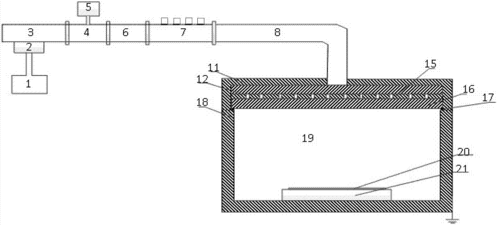
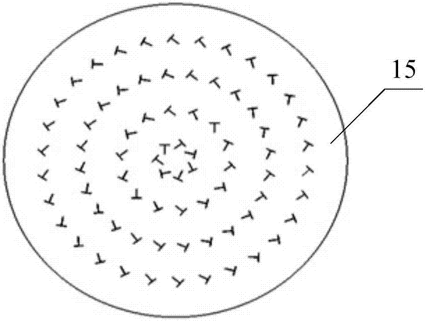
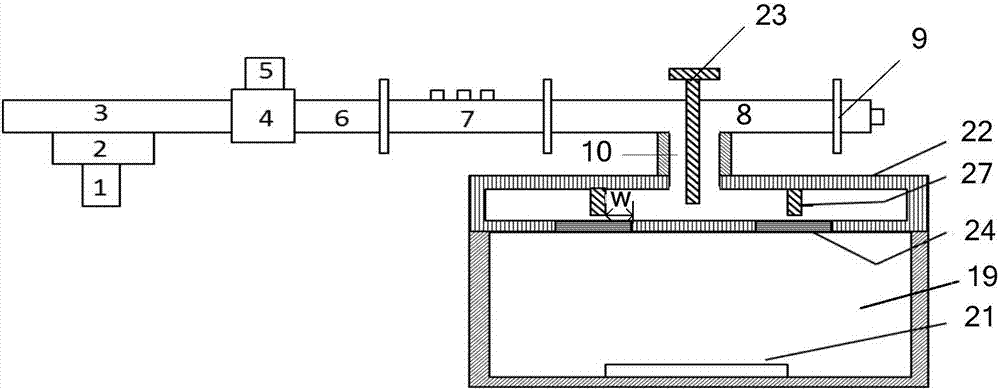
[0047] like figure 2 As shown, the present invention provides a surface wave plasma device, which includes: a microwave generating device, a microwave transmission matching structure and a vacuum chamber 19 . Among them, the microwave generating device is used to generate microwaves, including: microwave source power supply 1, microwave source 2 and resonator 3, microw...


PUM


Abstract

The invention provides a surface wave plasma device. A connection cavity is used to connect a resonant cavity and a rectangular waveguide. A screw probe extends into the resonant cavity via the rectangular waveguide and the connection cavity, so that microwave energy is fed in the connection cavity and the resonant cavity. By arranging a plurality of quartz windows in the bottom wall of the resonant cavity, the electric field of a standing wave formed in the resonant cavity by a microwave, and plasma is activated in the vacuum cavity. The plurality of quartz windows are equal to a plurality of plasma sources, which achieves uniformization of the plasma in the vacuum cavity in a large area compared with the conventional single plasma source, so as to meet the processing requirement for large-scale wafers.

Description

technical field [0001] The invention relates to the technical field of semiconductor equipment manufacturing, in particular to a surface wave plasma device. Background technique [0002] In recent years, with the rapid development of electronic technology, the general trend of people's requirements for integrated circuits tends to be highly integrated and larger area, which requires companies that produce integrated circuits to continuously improve the processing capacity of semiconductor wafers. Plasma devices are irreplaceable in the manufacturing process of integrated circuits (IC) or MEMS (Micro-Electro-Mechanical System, micro-electro-mechanical systems), therefore, the research and development of high-performance plasma generation equipment is crucial to the development of semiconductor manufacturing processes important. When the plasma equipment is used in the semiconductor manufacturing process, the most important consideration factor is: a large area of ​​uniform p...

Claims


Application Information

Patent Timeline
Patent Type & Authority Applications(China)
IPC IPC(8): H05H1/46
CPCH05H1/46H05H1/4615H01J37/32229H01J37/32238
Inventor 昌锡江区琼荣韦刚黄亚辉
Owner BEIJING NAURA MICROELECTRONICS EQUIP CO LTD
Why Eureka
Try Eureka