Electrostatic discharge protection structure in semiconductor device and semiconductor device

An electrostatic discharge protection, semiconductor technology, applied in the direction of semiconductor devices, semiconductor/solid-state device components, electric solid-state devices, etc., can solve the problems of small withstand current, burnout of protective structure, etc., to achieve increased withstand current, reduced Rdson, On-resistance reduction effect

Active Publication Date: 2017-12-15
INNOGRATION SUZHOU
View PDF1 Cites 0 Cited by
  • Summary
  • Abstract
  • Description
  • Claims
  • Application Information

AI Technical Summary

Problems solved by technology

If the maximum withstand current Imax of the tube is small, then the protective structure is also easily burned
[0007] Therefore, in the prior art, breakdown voltage and withstand current have become a pair of irreconcilable quantities

Method used


Image

  • Electrostatic discharge protection structure in semiconductor device and semiconductor device
  • Electrostatic discharge protection structure in semiconductor device and semiconductor device
  • Electrostatic discharge protection structure in semiconductor device and semiconductor device

Examples


Embodiment Construction

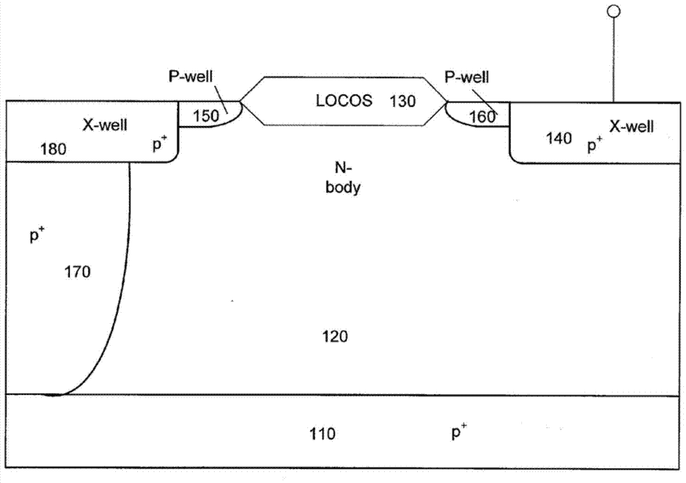
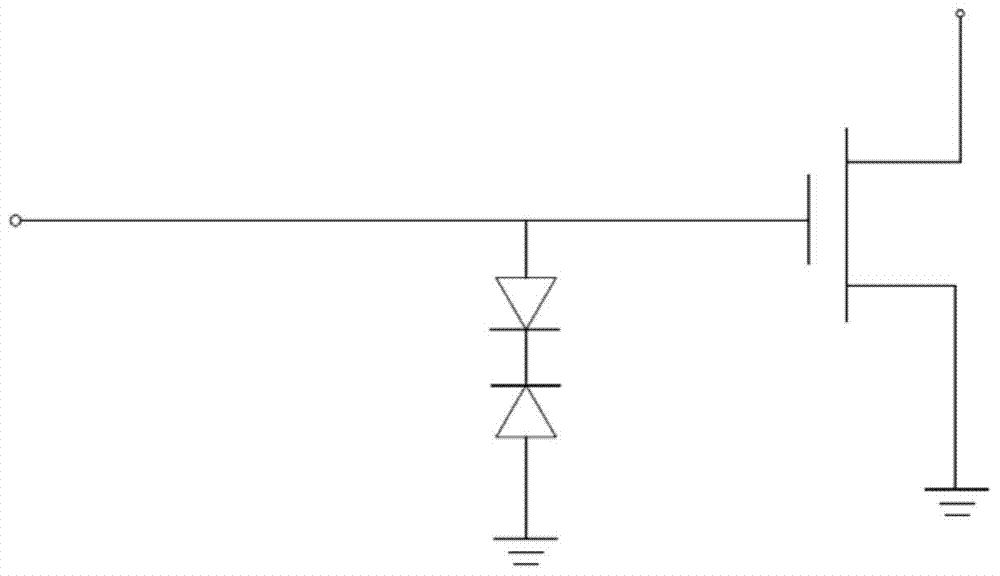
[0029] As mentioned in the background art, an existing ESD protection structure of a semiconductor device is realized by arranging a pair of back-to-back diodes. The working principle of this ESD protection structure is that when the externally applied voltage is greater than the breakdown voltage of one of the diodes, the ESD protection structure works in a conduction mode, and the external voltage is derived from the branch where the ESD protection structure is located. In this case, the breakdown voltage of each diode is proportional to the on-resistance Rdson when the structure turns on. In order to achieve the protection voltage required by the device, in the prior art, a thick field oxide layer is formed between the two P-well regions to increase the resistance value of Rdson, thereby increasing the breakdown voltage. However, this method of increasing the on-resistance will reduce the withstand current of the EDS protection structure, causing the ESD protection structur...


PUM


Abstract

An electrostatic discharge protection structure of a semiconductor device and a semiconductor device, the electrostatic discharge protection structure has a pair of back-to-back diodes, a field plate is always grounded above one of the diode junction regions, and the field plate and the N-type channel region are used The internal electric field between them increases the depletion layer in the junction region to increase the breakdown voltage. At the same time, because there is no field oxide layer, the on-resistance Rdson decreases, so that the withstand current value also increases. , effectively solve the contradiction between breakdown voltage and withstand current.

Description

technical field [0001] The invention belongs to the field of semiconductor device production, in particular to a semiconductor device with an electrostatic protection structure. Background technique [0002] Static electricity exists all the time in nature. When the external environment of the chip or the static charge accumulated inside the chip flows into or out of the chip through the pins of the chip, the instantaneous current (peak value can reach several amperes) or voltage will damage the integrated circuit. circuit, making the chip function invalid. With the development of the semiconductor industry, the feature size is further reduced, the component density is increasing, and the electronic components are more likely to suffer from electrostatic damage. Industrial electronic devices must be designed with qualified electrostatic protection. [0003] Among power amplifier devices, high-power devices such as VDMOS, LDMOS, and IGBT can withstand high voltage, and the m...

Claims


Application Information

Patent Timeline
Patent Type & Authority Patents(China)
IPC IPC(8): H01L23/60H01L27/02
Inventor 马强
Owner INNOGRATION SUZHOU
Why Eureka
Try Eureka