Schottky diode

A Schottky diode and Schottky contact technology, applied in electrical components, circuits, semiconductor devices, etc., can solve the problems of limited high voltage withstand capability, high reverse bias voltage, and inability to provide, to achieve improved withstand voltage capability, Effects of high reverse withstand voltage capability and low on-state power consumption

Inactive Publication Date: 2013-04-10
SHANGHAI HUAHONG GRACE SEMICON MFG CORP
View PDF4 Cites 0 Cited by
  • Summary
  • Abstract
  • Description
  • Claims
  • Application Information

AI Technical Summary

Problems solved by technology

Among them, although the Schottky diode can provide a relatively small on-resistance, its ability to withstand high voltage is limited, and it cannot provide a high reverse bias voltage.
In general applications, high-voltage diodes generally use PN junction diodes. The disadvantage is that the larger the reverse bias voltage is, the wider the required breakdown resistance depletion layer width will be. The larger the resistance, the overall performance of the device will be affected

Method used


Image

  • Schottky diode

Examples


Embodiment Construction

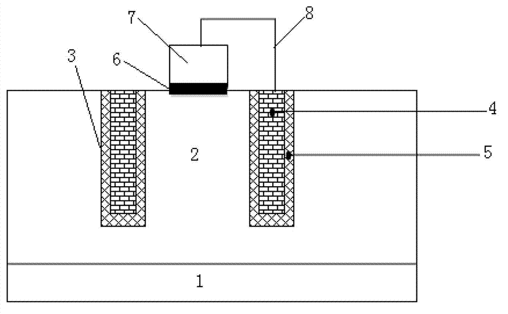
[0023] Such as figure 1 As shown, the Schottky diode of the present invention includes: an N-type epitaxial 2 on an N-type substrate 1, a deep trench 3 in the N-type epitaxial 2, a silicon dioxide layer 4 in the deep trench 3, and a deep trench There is a polysilicon region 5 inside the silicon dioxide layer 4 in the trench 3, a Schottky contact region 6 above the N-type epitaxy 2 between the deep trenches 3, a metal layer 7 on the Schottky contact region 6, and a polysilicon region 5 and the metal layer 7 are connected by a metal wire 8, wherein the thickness of the silicon dioxide layer 4 is greater than 1000 angstroms, the depth of the deep trench 3 is greater than 4um, and the metal layer is titanium metal.

[0024] With the increase of the thickness of the silicon dioxide layer 4, the withstand voltage capability of the present invention increases accordingly, and the ratio of the thickness of the silicon dioxide layer to the withstand voltage capability of the present in...


PUM

PropertyMeasurementUnit
Thicknessaaaaaaaaaa

Abstract

The invention discloses a schottky diode which comprises an N-type epitaxy arranged on an N-type substrate and deep grooves formed in the N-type epitaxy. A silica layer is arranged in each deep groove and a polycrystalline silicon area is arranged at the inner side of the silica layer. A schottky contact area is arranged on the N-type epitaxy between deep grooves, and a metal layer is arranged on the schottky contact area, wherein the depth of the silica layer is larger than 1000 angstroms and the polycrystalline silicon area is connected with the metal layer through a metal wire. When the depth of silica layer filling each deep groove is larger than 1000 angstroms, the schottky diode can endure the high pressure of over 80 V.

Description

technical field [0001] The invention relates to the field of semiconductor manufacturing, in particular to a Schottky diode. Background technique [0002] The traditional PN junction diode is in a single crystal semiconductor, part of which is doped with acceptor impurities is P-type semiconductor, and the other part is doped with donor impurities is N-type semiconductor, and the transition near the interface between P-type semiconductor and N-type semiconductor The region is called a PN junction, and a space charge layer is formed on both sides of its interface, and a self-built electric field is built. When there is no applied voltage, the diffusion current caused by the carrier concentration difference on both sides of the PN junction is equal to the drift current caused by the self-built electric field, and is in a state of electrical balance; when there is a forward voltage bias outside, the external electric field and the self-built electric field The mutual suppressi...

Claims


Application Information

Patent Timeline
IPC IPC(8): H01L29/872H01L29/06
Inventor 王飞
Owner SHANGHAI HUAHONG GRACE SEMICON MFG CORP
Why Eureka
Try Eureka