

Fin-type super junction power semiconductor transistor and preparation method thereof
A technology for power semiconductors and transistors, which is applied in the field of fin-type super-junction power semiconductor transistors and their preparation, and can solve problems such as failure to achieve
- Summary
- Abstract
- Description
- Claims
- Application Information
AI Technical Summary
Problems solved by technology
Method used
Image

Examples
Embodiment 1
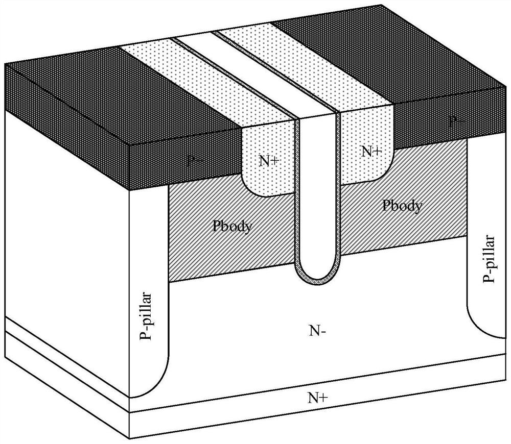
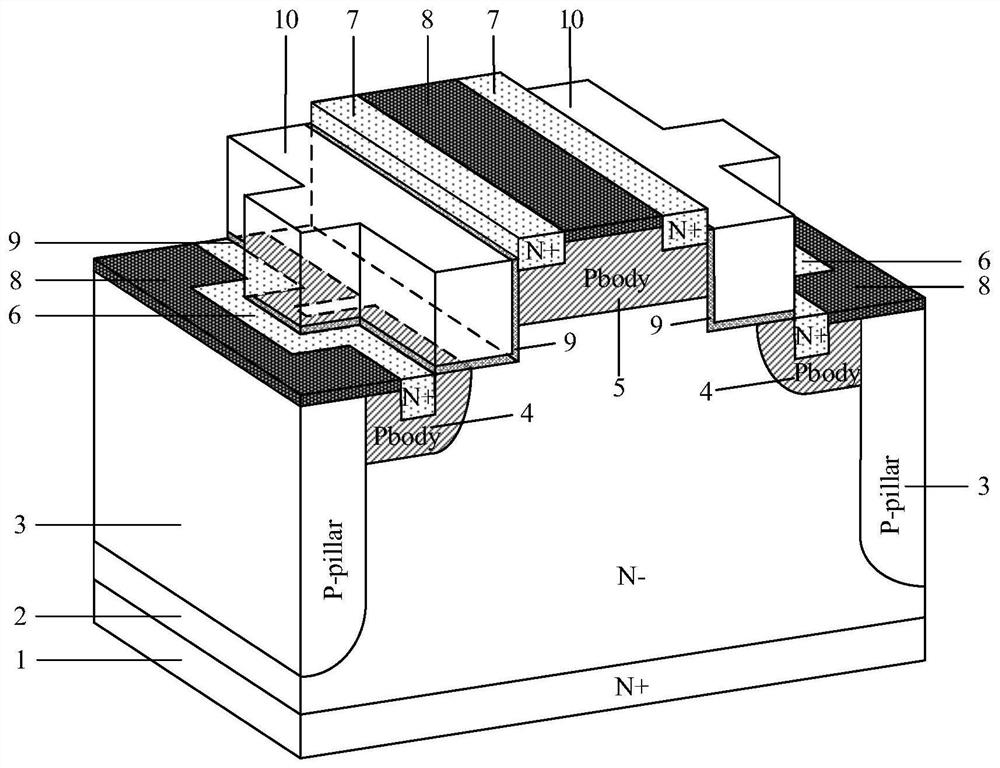
[0027] Combine below figure 2 , the present invention is described in detail, a fin-type super junction power semiconductor transistor, comprising: an N-type substrate 1, an N-type epitaxial layer 2 is arranged on the N-type substrate 1, and both sides of the N-type epitaxial layer 2 Columnar first P-type body regions 3 are respectively provided, and second P-type body regions 4 are respectively provided on both sides of the N-type epitaxial layer 2. The columnar first P-type body regions 3 and the second P-type body regions on the same side Type body region 4 touches each other, a first N-type heavily doped source region 6 is provided on the surface of the second P-type body region 4, a third P-type body region 5 is provided on the top of the N-type epitaxial layer 2, and a third P-type body region 5 is provided on the surface of the second P-type body region 4. Both ends of the surface of the P-type body region 5 are respectively provided with second N-type heavily doped so...
Embodiment 2
[0029] Combine below Figure 3 ~ Figure 8 , the present invention is described in detail, a method for preparing a fin-type super-junction power semiconductor transistor:
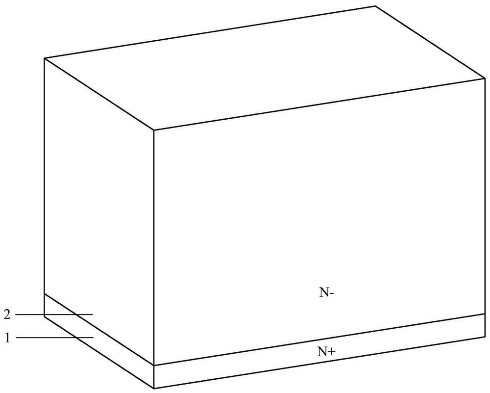
[0030] The first step: first select N-type silicon material as the substrate and epitaxially grow N-type epitaxial layer;
[0031] Step 2: use a mask to selectively etch a deep trench on the N-type epitaxial layer, and backfill the P-type material to form a columnar first P-type body region;
[0032] Step 3: selectively etching the N-type epitaxial layer to form a stepped epitaxial layer;
[0033] Step 4: using a mask to selectively implant boron into the stepped N-type epitaxial layer, and form a second P-type body region and a third P-type body region after annealing;
[0034] Step 5: Use a mask to selectively implant ions of arsenic or phosphorus on the surface of the second P-type body region to form a convex N-type heavily doped source region, and selectively implant ions of arsenic or phosphorus on ...
PUM
 Abstract
Description
Claims
Application Information