Leadless semiconductor package and manufacturing method thereof

a technology of leadless semiconductors and manufacturing methods, applied in semiconductor devices, semiconductor/solid-state device details, electrical apparatus, etc., can solve the problems of not meeting the high-performance dissipation requirements of automotive, industrial, commercial applications, and the limit of traditional lead frame packages, and achieves low electrical on-resistance.

Active Publication Date: 2006-05-30
ADVANCED SEMICON ENG INC
View PDF10 Cites 69 Cited by
  • Summary
  • Abstract
  • Description
  • Claims
  • Application Information

AI Technical Summary

Benefits of technology

[0011]The package of the present invention can be mounted onto a PC board with the die pads soldered directly to a matching thermal land on the PC board thereby providing a low thermal-impedance path to carry heat generated from the semiconductor devices mounted on the die pads. The use of 10–20 mils thick die pads and heavy gauge aluminum bond wires helps transfer heat from the package while providing low electrical on-resistance.

Problems solved by technology

However, as integrated circuits products move its endless pace toward both a faster speed and a smaller size, the traditional lead frame packages have become gradually obsolete for some high performance-required packages.
Traditional lead frame package has its limit of providing a solution for chip scale and low profile package due to the long inner leads and outer leads.
However, currently available leadless packages fail to meet the high power dissipation requirements of automotive, industrial, and commercial applications.

Method used


Image

  • Leadless semiconductor package and manufacturing method thereof
  • Leadless semiconductor package and manufacturing method thereof
  • Leadless semiconductor package and manufacturing method thereof

Examples


Embodiment Construction

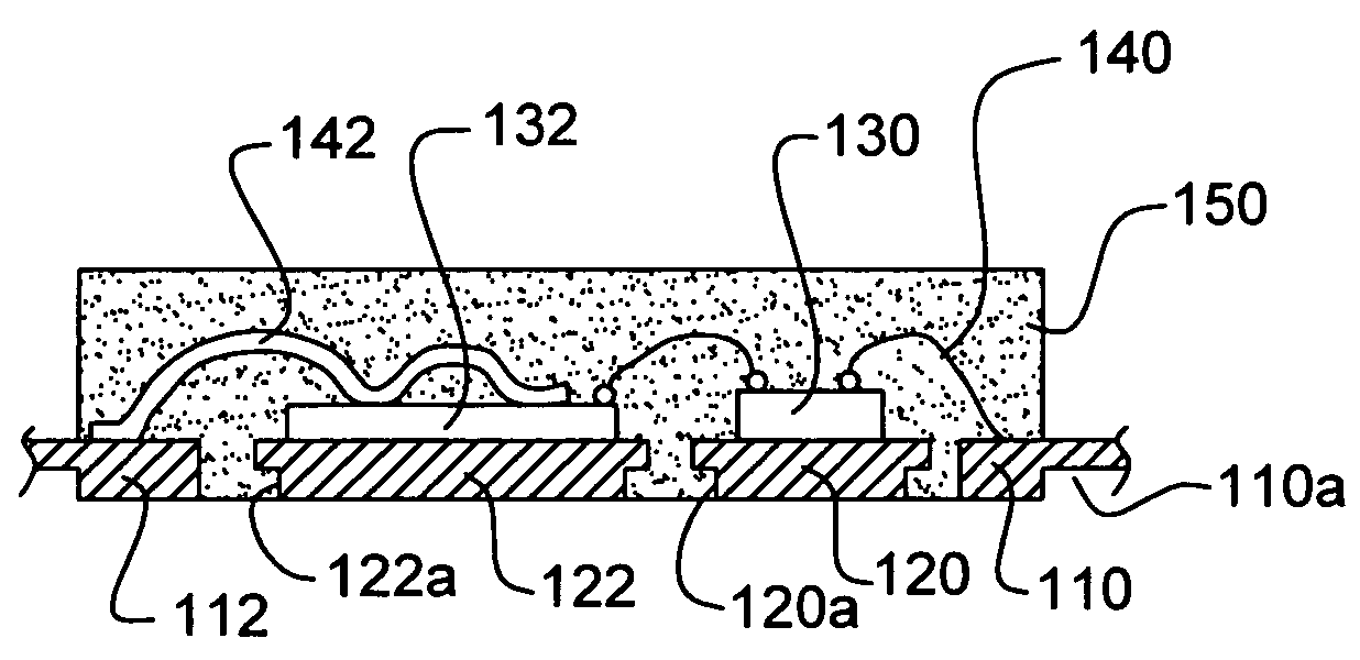
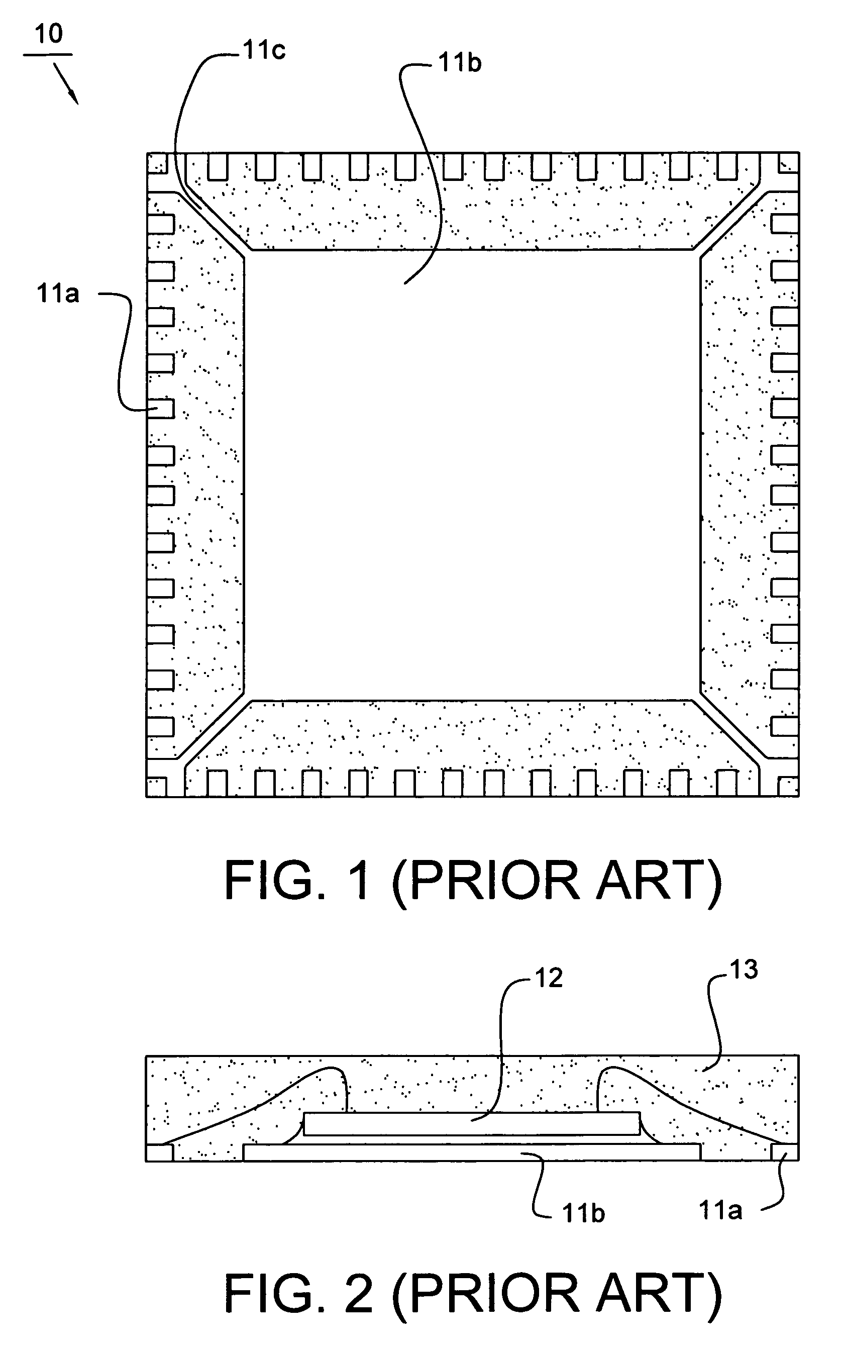
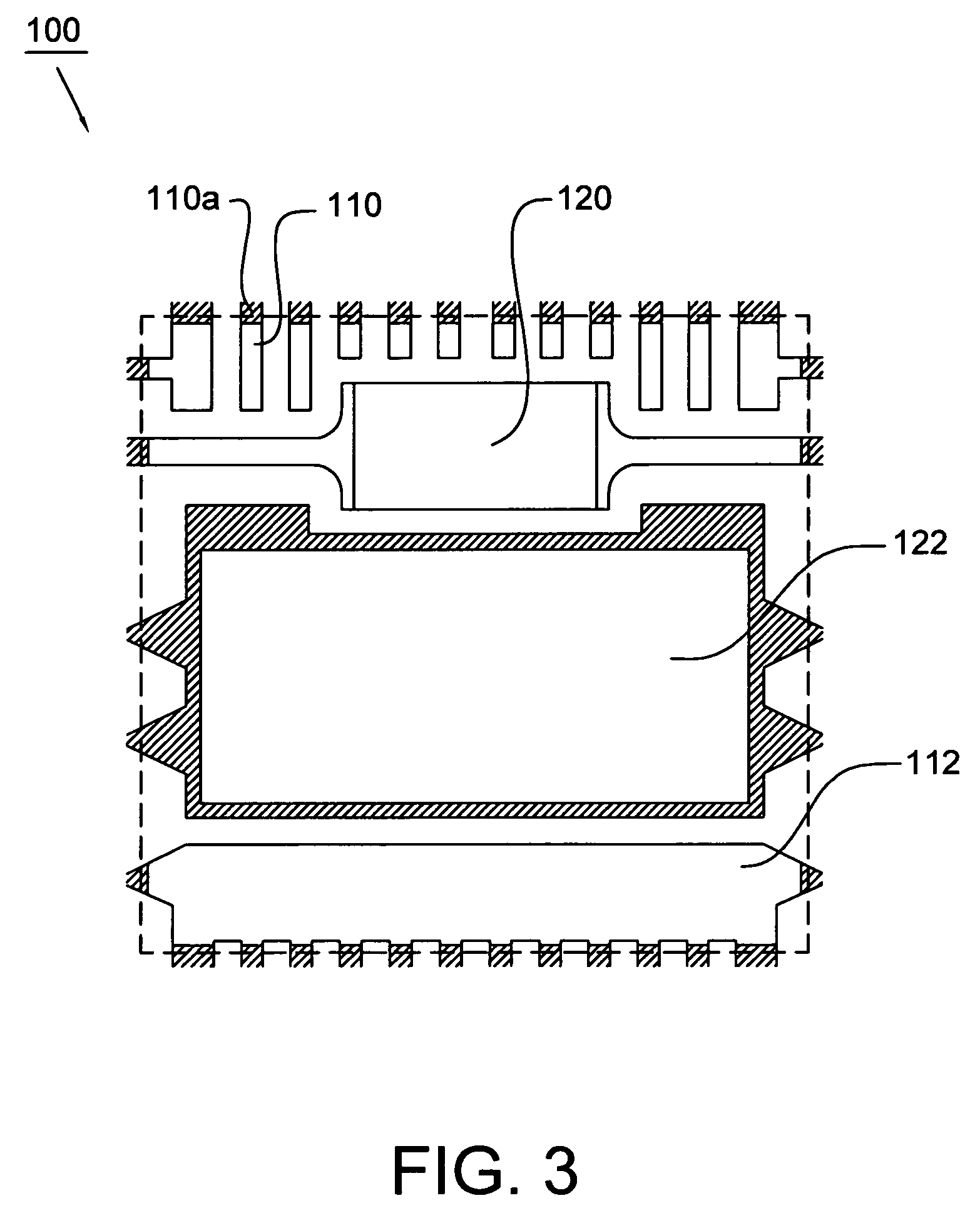
[0019]FIG. 3 shows a top plan view of a portion of a lead frame 100 according to one embodiment of the present invention. The lead frame 100 comprises a plurality of units separated from each other by a plurality of dambars (not shown). Though only one unit of the lead frame 100 is shown in FIG. 3, a lead frame for use with the invention can include any numbers of units that is compatible with the manufacturing equipment, e. g., mold, being used. The dambars generally form an orthogonal grid on the lead frame 100. The lead frame 100 is typically made of a copper-base alloy or made of copper or alloys containing copper. The lead frame 100 have a thickness between about 10 mils and about 20 mils, and is shaped by etching in the manner that each unit of the lead frame 100 has a plurality of leads 110 and a power output bar 112 arranged about the periphery of two die pads 120 and 122. In addition, a half-etched operation is conducted in the manufacturing process of the lead frame 100. T...


PUM


Abstract

A leadless semiconductor package mainly includes a semiconductor device securely attached to an upper surface of a die pad by solder paste and a plurality of leads arranged about the periphery of the die pad. The thickness of the leads and the die pad are within a range of 10 to 20 mils. The semiconductor device is electrically coupled to one of the leads. A package body is formed over the semiconductor device and the leads in a manner that the lower surfaces of the die pad and the leads are exposed through the package body. Preferably, the first semiconductor device is electrically coupled to one of the leads by at least one heavy gauge aluminum wire. The present invention further provides a method of producing the semiconductor package described above.

Description

BACKGROUND OF THE INVENTION[0001]1. Field of the Invention[0002]This invention relates to lead frame packages, and more specifically to leadless semiconductor packages and manufacturing methods thereof.[0003]2. Description of the Related Art[0004]Lead frame packages have been used for a long period of time in the IC packaging history mainly because of their low manufacturing cost and high reliability. However, as integrated circuits products move its endless pace toward both a faster speed and a smaller size, the traditional lead frame packages have become gradually obsolete for some high performance-required packages. Thus BGA (Ball Grid Array Packages) and CSP (Chip Scale Package) have emerged and become increasingly popular as a new packaging choice. The former has been widely used in IC chips that have higher I / Os and need better electrical and thermal performance than the conventional packages such as CPU and graphic chips. The latter has been widely used in mobile products of ...

Claims


Application Information

Patent Timeline
Patent Type & Authority Patents(United States)
IPC IPC(8): H01L23/495H01L23/31
CPCH01L23/3107H01L23/4952H01L23/49562H01L23/49575H01L24/40H01L24/48H01L24/49H01L24/73H01L23/49548H01L24/45H01L2224/32245H01L2224/45124H01L2224/45144H01L2224/48091H01L2224/48137H01L2224/48247H01L2224/48472H01L2224/48599H01L2224/48699H01L2224/4903H01L2224/49051H01L2224/73265H01L2224/85205H01L2924/01005H01L2924/01006H01L2924/01013H01L2924/01028H01L2924/01029H01L2924/01046H01L2924/01047H01L2924/0105H01L2924/01051H01L2924/01078H01L2924/01079H01L2924/01082H01L2924/01083H01L2924/014H01L2924/14H01L2924/3011H01L2924/01033H01L2924/01076H01L2224/73221H01L2224/40247H01L2924/00014H01L2924/00H01L2924/181H01L2224/83801H01L2224/8385H01L2224/05639H01L2224/0603H01L2224/05554H01L2224/05552H01L2224/4846H01L2224/49113H01L2224/45015H01L2924/00012H01L2224/85399H01L2924/2076H01L2224/40091
Inventor KOH, KWANG WONKIM, SONG WOONPARK, SANG BAE
Owner ADVANCED SEMICON ENG INC
Why Eureka
Try Eureka