Touch display screen

A touch display and touch electrode technology, applied in optics, instruments, electrical digital data processing, etc., can solve the problems of increasing the thickness and weight of electronic products, increasing product production costs, complex assembly processes, etc., to save materials and Assembly cost, reduced production cost, and simple process

Active Publication Date: 2014-12-24
NANCHANG VIRTUAL REALITY RES INST CO LTD
View PDF5 Cites 4 Cited by
  • Summary
  • Abstract
  • Description
  • Claims
  • Application Information

AI Technical Summary

Problems solved by technology

[0004] As a combined module of polarizers, filters, liquid crystal modules, and TFT (Thin Film Transistor, thin film transistor) modules, the display screen has a relatively large thickness. At the same time, it not only requires a complex assembly process, but also increases the thickness and weight of the electronic product again. Furthermore, one more assembly process means increasing the probability of product failure and greatly increasing the production cost of the product.

Method used


Image

  • Touch display screen
  • Touch display screen
  • Touch display screen

Examples


Embodiment Construction

[0025] The touch display screen will be further described below in conjunction with the accompanying drawings and specific embodiments.

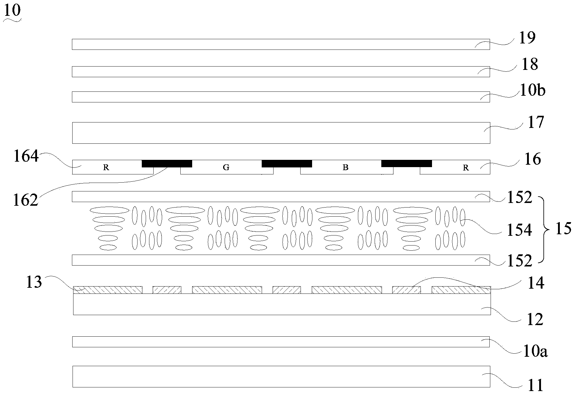
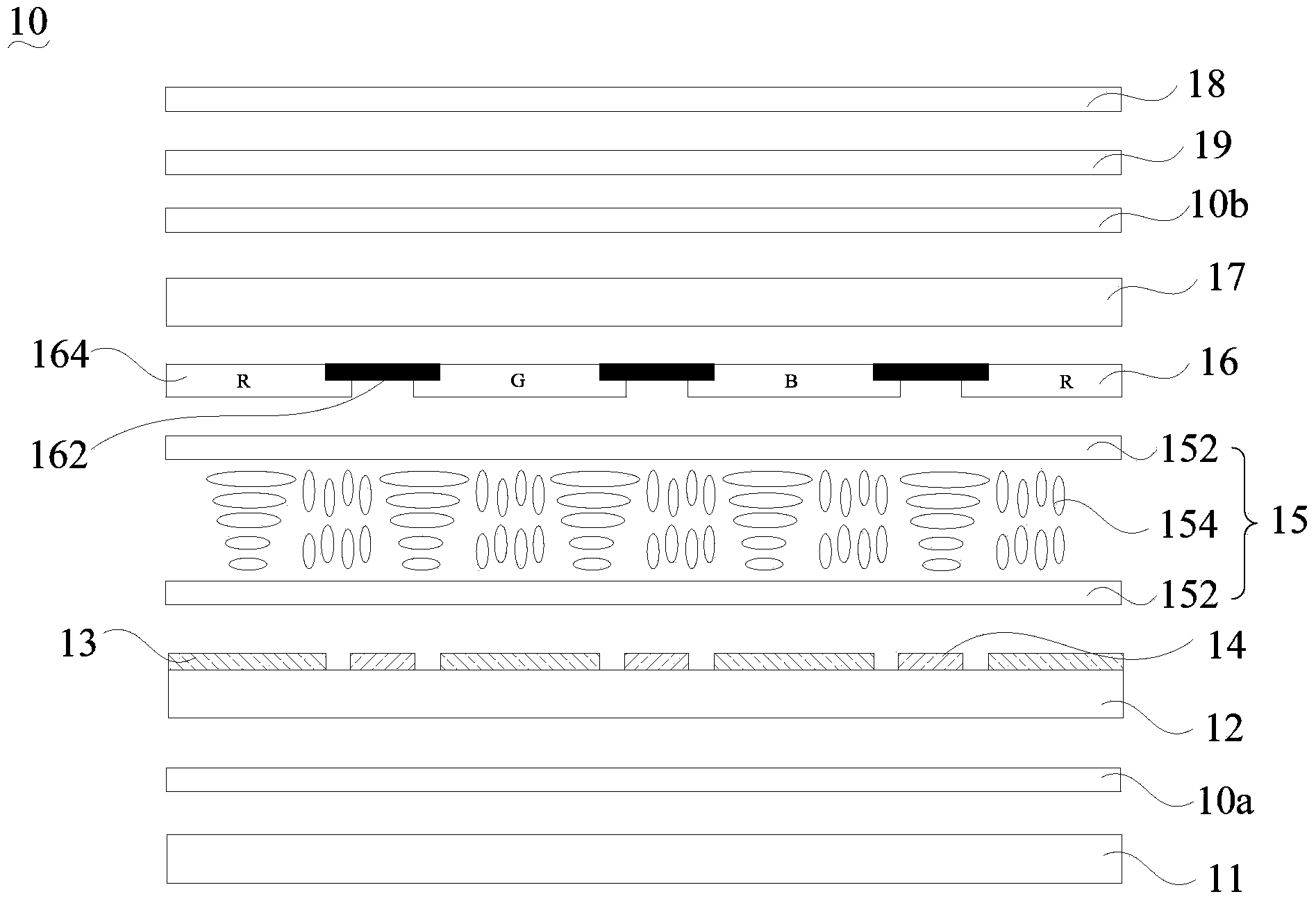
[0026] Such as figure 1 As shown, the touch display screen 10 of one embodiment includes a lower polarizer (second polarizer) 11, a first substrate 12, a TFT electrode 13, a common electrode 14, a liquid crystal module 15, a filter layer 16, and a second substrate 17. A transparent conductive layer 18 and an upper polarizer (first polarizer) 19 .

[0027] The lower polarizer 11 , the first substrate 12 , the liquid crystal module 15 , the filter layer 16 , the second substrate 17 and the upper polarizer 19 are stacked sequentially from bottom to top.

[0028] The liquid crystal module 15 includes two alignment films 152 disposed opposite to each other and a liquid crystal layer 154 sandwiched between the two alignment films 152 .

[0029] The TFT electrodes 13 are disposed on the surface of the first substrate 12 close to the liquid crysta...


PUM

PropertyMeasurementUnit
thicknessaaaaaaaaaa
thicknessaaaaaaaaaa
thicknessaaaaaaaaaa

Abstract

The invention provides a touch display screen, which comprises a first substrate, a liquid crystal module, a filter layer, a second substrate and a first polaroid, wherein the first substrate, the liquid crystal module, the filter layer, the second substrate and the first polaroid are stacked in sequence; the surface, near one side of the liquid crystal module, of the first substrate is provided with a plurality of mutually insulated TFT (thin film transistor) electrodes and a plurality of mutually insulated common electrodes; the common electrodes and the TFT electrodes are alternately arranged in an insulation manner; the TFT electrodes and the common electrodes are matched to control the arrangement state of liquid crystal molecules in the liquid crystal module; the touch display screen also comprises a transparent conducting layer arranged on the surface, backing on to one side of the liquid crystal module, of the second substrate or the surface of the first polaroid; the transparent conducting layer comprises a matrix and conducting nanometer wires filled in the matrix; the matrix is solidified transparent photosensitive resin; the transparent conducting layer is patterned to form a plurality of mutually insulated touch electrodes; the touch electrodes are matched with the common electrodes to form a double-layer touch induction structure, and the double-layer touch induction structure is used for determining coordinates of a touch point. The touch display screen has the characteristics of being thin and low in production cost.

Description

technical field [0001] The invention relates to the technical field of electronic products, in particular to a touch display screen. Background technique [0002] A touch screen is an inductive device that receives touch input signals. The touch screen has endowed information interaction with a new look and is a very attractive new information interaction device. The development of touch screen technology has aroused widespread concern in the information media circles at home and abroad, and has become a rising high-tech industry in the optoelectronic industry. [0003] At present, electronic products with a touch display function include a display screen and a touch screen located on the display screen. However, as a component independent of the display screen, the touch screen needs to be used according to the display screen when it is used in some electronic products that realize human-computer interaction. The size of the order is ordered, and then assembled. There are...

Claims


Application Information

Patent Timeline
Patent Type & Authority Applications(China)
IPC IPC(8): G06F3/044G02F1/1333
Inventor 刘伟唐根初蒋芳
Owner NANCHANG VIRTUAL REALITY RES INST CO LTD
Why Eureka
Try Eureka