Waveguide structure based on artificial surface plasmon device and amplifier

An artificial surface plasmon and waveguide structure technology, applied in waveguides, electrical components, waveguide-type devices, etc., can solve the problems of limitation, redundancy, and difficulty in integrating active chips, and achieve light weight, simple adjustment, and strong sub-wavelength. Effects of Effects and Field Local Effects

Active Publication Date: 2015-02-04
SOUTHEAST UNIV
View PDF3 Cites 32 Cited by
  • Summary
  • Abstract
  • Description
  • Claims
  • Application Information

AI Technical Summary

Problems solved by technology

[0004] The single-layer artificial surface polariton structure that has been reported, due to the limitation of its structure size, if it is directly used in the microwave frequency band, it is redundant and cannot give full play to its special physical properties.
And because most of this structure is a single conductor structure, it is difficult to integrate active chips on this structure.
According to the existing reports, the surface plasmon and guided wave conversion device proposed for this structure, because it needs to add two large-area tapered coplanar waveguide structures, is not suitable for practical large-scale circuit design. larger limit

Method used


Image

  • Waveguide structure based on artificial surface plasmon device and amplifier
  • Waveguide structure based on artificial surface plasmon device and amplifier
  • Waveguide structure based on artificial surface plasmon device and amplifier

Examples


Embodiment Construction

[0025] The technical solution of the present invention will be described in detail below in conjunction with the accompanying drawings.

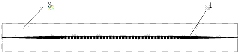
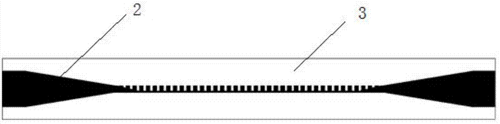
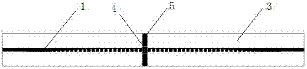
[0026] like figure 1 and figure 2 As shown, a waveguide structure based on an artificial surface plasmon device of the present invention includes a dielectric layer 3 , and a first metal sheet 1 and a second metal sheet 2 fixedly connected to both sides of the dielectric layer 3 and facing each other. Periodically arranged grooves are respectively arranged on the first metal sheet 1 and the second metal sheet 2 , and the opening direction of the grooves on the first metal sheet 1 is opposite to the opening direction of the grooves on the second metal sheet 2 . The grooves on the first metal sheet 1 and the second metal sheet 2 are comb-shaped. The depths of the grooves located in the middle of the first metal sheet 1 are equal, and the depths of the grooves located at both ends of the first metal sheet 1 gradually increase from the end to...


PUM

PropertyMeasurementUnit
dielectric lossaaaaaaaaaa

Abstract

The invention discloses a waveguide structure based on an artificial surface plasmon device. The waveguide structure comprises a dielectric layer, a first metal sheet and a second metal sheet, the first metal sheet and the second metal sheet are oppositely and fixedly connected on two sides of the dielectric layer, periodically arranged grooves are formed in the first metal sheet and the second metal sheet respectively, the depths of the grooves positioned in the middles of the metal sheets are equal, and the depths of the grooves positioned in two ends of each metal sheet are gradually increased from the end to the middle respectively until the depths are equal to the depths of the grooves positioned in the middles of the metal sheets. Novel artificial surface plasmon units are specifically arranged to form the waveguide structure, a curved surface arch circuit is conveniently manufactured, and the waveguide structure has a high practical value. The invention further provides an amplifier of the waveguide structure based on the artificial surface plasmon device, and the amplifier can amplify an artificial surface plasmon wave in a wide frequency band.

Description

technical field [0001] The invention relates to an artificial electromagnetic material, in particular to a waveguide structure and an amplifier based on an artificial surface plasmon device. Background technique [0002] New artificial electromagnetic materials (Metamaterials) are electromagnetic materials that can be artificially designed to meet specific requirements of equivalent dielectric constant and magnetic permeability. The new artificial electromagnetic material is proposed based on the equivalent medium theory, and the artificial composite structure of the equivalent dielectric constant and permeability can be changed by changing the size of the unit structure of the new artificial electromagnetic material. After more than ten years of development, new artificial electromagnetic materials have achieved rapid development, and have been widely used in stealth and antenna engineering. [0003] In recent years, the structure based on surface plasmon polaritons has be...

Claims


Application Information

Patent Timeline
Patent Type & Authority Applications(China)
IPC IPC(8): H01P3/02
Inventor 崔铁军张浩驰刘硕沈晓鹏陈林辉李连鸣
Owner SOUTHEAST UNIV
Why Eureka
Try Eureka