

Target blasting fixture and target blasting method
A target material and sandblasting technology, which is used in manufacturing tools, abrasive jet machine tools, used abrasive treatment devices, etc. The effect of sandblasting efficiency, ensuring sandblasting quality, and saving the cost of tape
- Summary
- Abstract
- Description
- Claims
- Application Information
AI Technical Summary
Problems solved by technology
Method used
Image

Examples
Embodiment Construction
[0034] As mentioned in the background section, the accuracy of blasting the sandblasting area in the target material through tape protection is poor, and the size of the sandblasting area is difficult to ensure, which affects the formation position of the reverse sputtering film. Moreover, when removing the tape beyond the sputtering area by blade cutting technology, it is easy to leave scratches on the sputtering surface, which affects the adhesion of the anti-sputtering film.
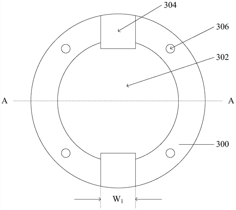
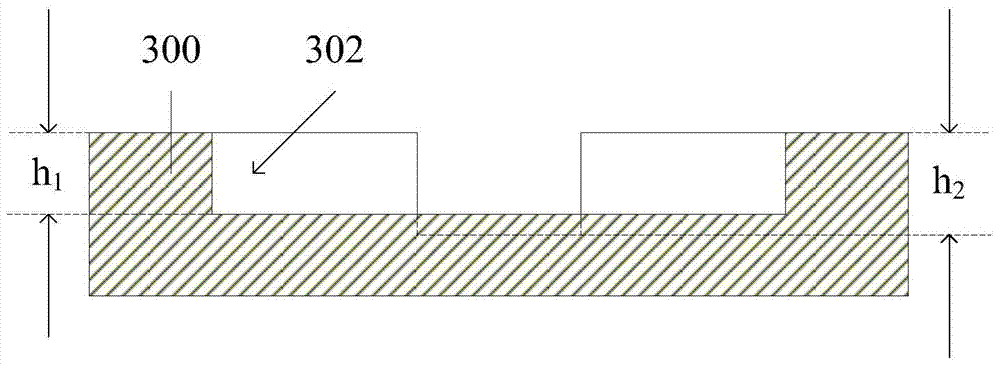
[0035] The invention provides a target sandblasting fixture comprising a target chuck, a cover plate and more than two connectors. Before sandblasting, the target is placed in the first groove of the target chuck, and The sputtering area of the target is opposite to the bottom surface of the first groove, and the cover plate is placed on the sputtering area of the target, and the first end of the connector is fixed on the target chuck outside the first groove , fix the second end of the connecting...
PUM
| Property | Measurement | Unit |
|---|---|---|
| thickness | aaaaa | aaaaa |
| diameter | aaaaa | aaaaa |
| thickness | aaaaa | aaaaa |
Abstract
Description
Claims
Application Information