Array substrate, touch display panel and touch display device

A technology of array substrates and electrode blocks, which is applied in the fields of instruments, calculations, and electrical digital data processing, etc., can solve problems such as display stripes and uneven display on the display screen, reduce voltage variation, improve display effects, and slow down coupling The effect of the degree of mutation

Active Publication Date: 2015-06-10
SHANGHAI TIANMA MICRO ELECTRONICS CO LTD +1
View PDF4 Cites 23 Cited by
  • Summary
  • Abstract
  • Description
  • Claims
  • Application Information

AI Technical Summary

Problems solved by technology

[0009] In view of this, the present invention provides an array substrate, a touch display panel, and a touch display device to solve the problems of uneven display and horizontal stripes on the display screen at the junction of electrode blocks in the prior art

Method used


Image

  • Array substrate, touch display panel and touch display device
  • Array substrate, touch display panel and touch display device
  • Array substrate, touch display panel and touch display device

Examples


Embodiment Construction

[0027] The following will clearly and completely describe the technical solutions in the embodiments of the present invention with reference to the accompanying drawings in the embodiments of the present invention. Obviously, the described embodiments are only some, not all, embodiments of the present invention. Based on the embodiments of the present invention, all other embodiments obtained by persons of ordinary skill in the art without making creative efforts belong to the protection scope of the present invention.

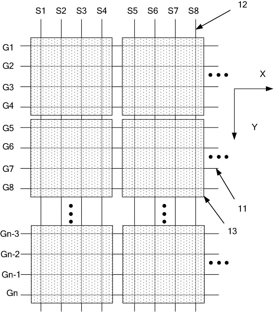
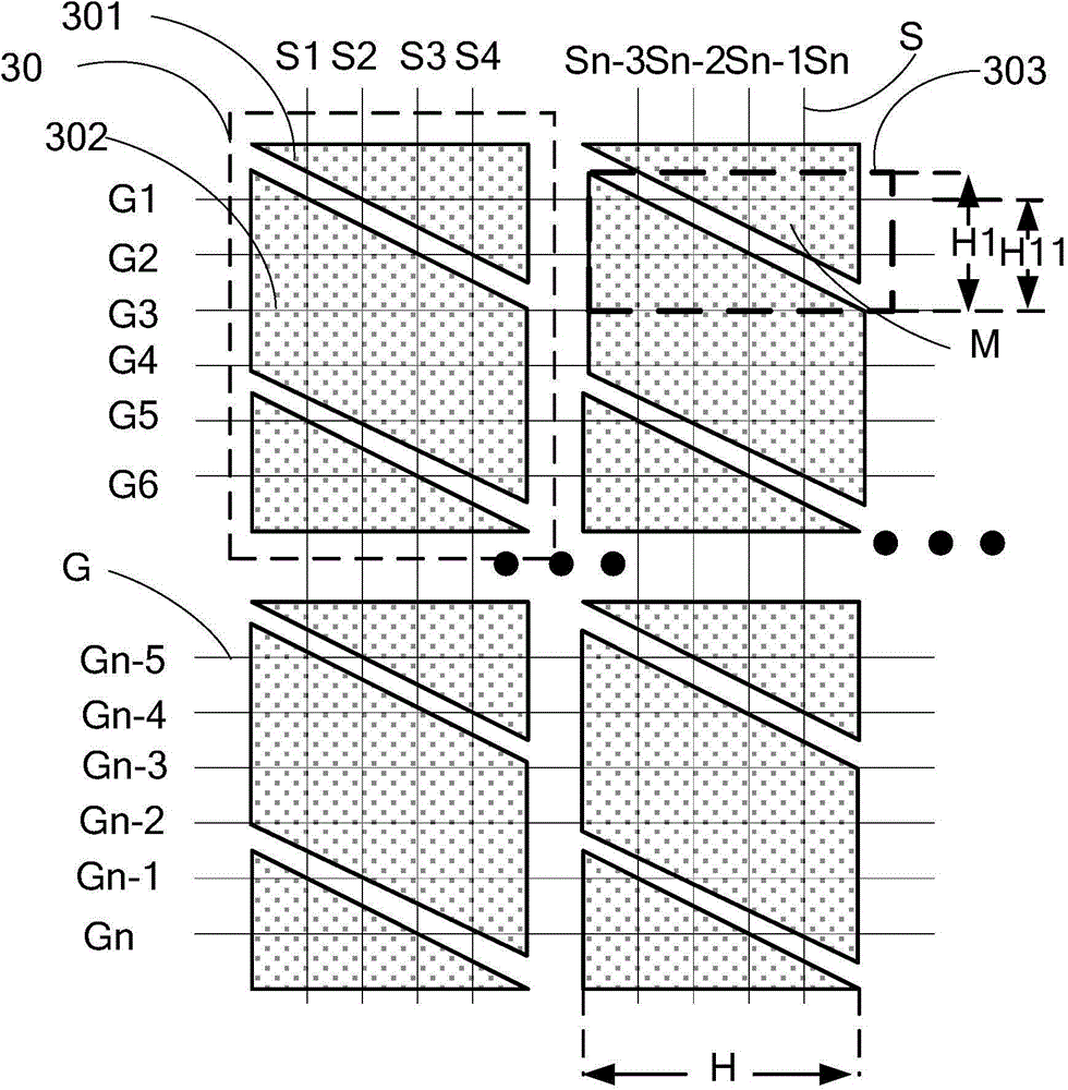
[0028] An embodiment of the present invention provides an array substrate, the array substrate includes a plurality of gate lines G1~Gn and a plurality of data lines S1~Sn, and a grid surrounded by the gate lines G1~Gn and data lines S1~Sn A plurality of pixel units, a common electrode layer, and a driving circuit, the common electrode layer is divided into a plurality of electrode units, the electrode units include at least two electrode blocks, and the two el...


PUM


Abstract

The invention provides an array substrate, a touch display panel and a touch display device. The array substrate comprises grid lines, data lines, pixel units and a public electrode layer, wherein the pixel units are enclosed by the grid lines and the data lines, and the public electrode layer is divided into multiple electrode units. Each electrode unit comprises at least two electrode blocks provided with nested intersection areas, the length of the intersection area in the extending direction of the data lines is larger than or equal to the length of an overlapped area of driving signals along the extending direction of the data lines, and the overlapped area of the driving signals comprises the overlapped grid lines and pixel units electrically connected with the grid lines. Accordingly, coupling mutation degree at the boundary of the adjacent electrode blocks can be lowered, voltage change amplitude of the electrode blocks during cutoff of thin-film transistors of the pixel units of the adjacent electrode block boundary is alleviated, and image display effect is improved.

Description

technical field [0001] The present invention relates to the field of touch technology, and more specifically, to an array substrate, a touch display panel and a touch display device. Background technique [0002] With the development of integrated touch and display technology, the common electrodes of the array substrate of the display panel can be reused as touch electrodes, and time-sequential touch driving and display driving can be performed in a time-sharing manner, so as to simultaneously realize touch and display. Display function. In this way, the touch electrodes are directly integrated into the display panel, which greatly reduces the manufacturing cost, improves the production efficiency, and reduces the thickness of the panel. [0003] Please refer to figure 1 , figure 1 It is a structural schematic diagram of an array substrate for a touch display panel, the array substrate includes: a plurality of gate lines 11, a plurality of data lines 12 and a common elec...

Claims


Application Information

Patent Timeline
Patent Type & Authority Applications(China)
IPC IPC(8): G06F3/041G06F3/044
CPCG06F3/0412G06F3/04164G06F3/0443G06F3/0448
Inventor 李嘉灵马从华姚绮君
Owner SHANGHAI TIANMA MICRO ELECTRONICS CO LTD
Why Eureka
Try Eureka